As filed with the Securities and Exchange Commission on April 11, 2024
UNITED STATES
SECURITIES AND EXCHANGE COMMISSION
Washington, D.C. 20549
FORM
REGISTRATION STATEMENT PURSUANT TO SECTION 12(b) OR 12(g) OF THE SECURITIES EXCHANGE ACT OF 1934 |
OR
ANNUAL REPORT PURSUANT TO SECTION 13 OR 15(d) OF THE SECURITIES EXCHANGE ACT OF 1934 |
For the fiscal year ended
OR
TRANSITION REPORT PURSUANT TO SECTION 13 OR 15(d) OF THE SECURITIES EXCHANGE ACT OF 1934 |
OR
SHELL COMPANY REPORT PURSUANT TO SECTION 13 OR 15(d) OF THE SECURITIES EXCHANGE ACT OF 1934 |
Date of event requiring this shell company report
Commission file number
南茂科技股份有限公司
(Exact Name of Registrant as Specified in Its Charter)
(Translation of Registrant’s Name into English)
(Jurisdiction of Incorporation or Organization)
(Address of Principal Executive Offices)
Vice President, Finance and Accounting Management Center
ChipMOS TECHNOLOGIES INC.
Telephone: +
Facsimile: +886-3-566-8970
(Name, Telephone, E-mail and/or Facsimile Number and Address of Company Contact Person)
Securities registered or to be registered pursuant to Section 12(b) of the Act:
Title of Each Class
|
Trading Symbol(s)
|
Name of Each Exchange on Which Registered
|
The |
Securities registered or to be registered pursuant to Section 12(g) of the Act:
None
(Title of Class)
Securities for which there is a reporting obligation pursuant to Section 15(d) of the Act:
None
(Title of Class)
Indicate the number of outstanding shares of each of the issuer’s classes of capital or common stock as of the close of the period covered by the annual report.
As of December 31, 2023,
Indicate by check mark if the registrant is a well-known seasoned issuer, as defined in Rule 405 of the Securities Act. Yes ☐
If this report is an annual or transition report, indicate by check mark if the registrant is not required to file reports pursuant to Section 13 or 15(d) of the Securities Exchange Act of 1934. Yes ☐
Indicate by check mark whether the registrant: (1) has filed all reports required to be filed by Section 13 or 15(d) of the Securities Exchange Act of 1934 during the preceding 12 months (or for such shorter period that the registrant was required to file such reports), and (2) has been subject to such filing requirements for the past 90 days.
Indicate by check mark whether the registrant has submitted electronically every Interactive Data File required to be submitted pursuant to Rule 405 of Regulation S-T (§232.405 of this chapter) during the preceding 12 months (or for such shorter period that the registrant was required to submit such files).
Indicate by check mark whether the registrant is a large accelerated filer, an accelerated filer, a non-accelerated filer, or an emerging growth company. See definition of “large accelerated filer”, “accelerated filer”, and “emerging growth company” in Rule 12b-2 of the Exchange Act. :
☒ |
Accelerated Filer |
☐ |
Non-Accelerated Filer |
☐ |
Emerging growth company |
If an emerging growth company that prepares its financial statements in accordance with U.S. GAAP, indicate by check mark if the registrant has elected not to use the extended transition period for complying with any new or revised financial accounting standards provided pursuant to Section 13(a) of the Exchange Act. ☐
Indicate by check mark whether the registrant has filed a report on and attestation to its management’s assessment of the effectiveness of its internal control over financial reporting under Section 404(b) of the Sarbanes-Oxley Act (15 U.S.C. 7262(b)) by the registered public accounting firm that prepared or issued its audit report.
If securities are registered pursuant to Section 12(b) of the Act, indicate by check mark whether the financial statements of the registrant included in the filing reflect the correction of an error to previously issued financial statements.
Indicate by check mark whether any of those error corrections are restatements that required a recovery analysis of incentive-based compensation received by any of the registrant’s executive officers during the relevant recovery period pursuant to §240.10D-1(b). ☐
Indicate by check mark which basis of accounting the registrant has used to prepare the financial statements included in this filing.
U.S. GAAP ☐ |
by the International Accounting Standards Board ☒ |
Other ☐ |
If “Other” has been checked in response to the previous question, indicate by check mark which financial statement item the registrant has elected to follow.
Item 17 ☐ Item 18 ☐
If this is an annual report, indicate by check mark whether the registrant is a shell company (as defined in Rule 12b-2 of the Exchange Act). Yes ☐ No
* Not for trading, but only in connection with the listing on the
TABLE OF CONTENTS
ChipMOS TECHNOLOGIES INC.
1 |
||
|
|
|
3 |
||
|
|
|
Item 1. |
3 |
|
|
|
|
Item 2. |
3 |
|
|
|
|
Item 3. |
3 |
|
|
|
|
Item 4. |
17 |
|
|
|
|
Item 4A. |
42 |
|
|
|
|
Item 5. |
42 |
|
|
|
|
Item 6. |
53 |
|
|
|
|
Item 7. |
58 |
|
|
|
|
Item 8. |
58 |
|
|
|
|
Item 9. |
59 |
|
|
|
|
Item 10. |
59 |
|
|
|
|
Item 11. |
72 |
|
|
|
|
Item 12. |
73 |
|
|
|
|
75 |
||
|
|
|
Item 13. |
75 |
|
|
|
|
Item 14. |
Material Modifications to the Rights of Security Holders and Use of Proceeds |
75 |
|
|
|
Item 15. |
75 |
|
|
|
|
Item 16A. |
76 |
|
|
|
|
Item 16B. |
76 |
|
|
|
|
Item 16C. |
76 |
|
|
|
|
Item 16D. |
76 |
|
|
|
|
Item 16E. |
Purchases of Equity Securities by the Issuer and Affiliated Purchasers |
76 |
|
|
|
Item 16F. |
76 |
|
|
|
|
Item 16G. |
76 |
|
|
|
|
Item 16H. |
79 |
|
|
|
|
Item 16I. |
Disclosure Regarding Foreign Jurisdictions that Prevent Inspections |
79 |
|
|
|
Item 16J. |
79 |
|
|
|
|
Item 16K. |
79 |
|
|
|
|
81 |
||
|
|
|
Item 17. |
81 |
|
|
|
|
Item 18. |
81 |
|
|
|
|
Item 19. |
81 |
|
CAUTIONARY STATEMENT FOR PURPOSES OF THE “SAFE HARBOR” PROVISIONS OF
THE PRIVATE SECURITIES LITIGATION REFORM ACT OF 1995
Except for historical matters, the matters discussed in this Annual Report on Form 20-F are forward-looking statements that are subject to a number of significant risks and uncertainties and are based on information as of the date hereof. These statements are generally indicated by the use of forward-looking terminology such as the words “anticipate”, “believe”, “estimate”, “expect”, “intend”, “may”, “plan”, “project”, “will”, “could”, “might”, “should” and other words and phrases of similar import that express an indication of actions or results of actions that may or are expected to occur in the future. These statements appear in a number of places throughout this Annual Report on Form 20-F and include statements regarding our intentions, beliefs or current expectations concerning, among other things, our results of operations, financial condition, liquidity, prospects, growth, strategies and the industries in which we operate.
By their nature, forward-looking statements involve risks and uncertainties because they relate to events and depend on circumstances that may or may not occur in the future. Forward-looking statements are not guarantees of future performance and our actual results of operations, financial condition and liquidity, and the development of the industries in which we operate may differ materially from those made in or suggested by the forward-looking statements contained in this Annual Report on Form 20-F. Important factors that could cause those differences include, but are not limited to:
The factors identified above are believed to be important factors (but not necessarily all of the important factors) that could cause actual results to differ materially from those expressed in any forward-looking statement made by us. Other factors not discussed herein could also have material adverse effects on us. All forward-looking statements included in this Annual Report on Form 20-F are expressly qualified in their entirety by the foregoing cautionary statements. We undertake no obligation to update any forward-looking statement (or its associated cautionary language), whether as a result of new information or future events.
Forward-looking statements include, but are not limited to, statements regarding our strategy and future plans, future business condition and financial results, our capital expenditure plans, our capacity expansion plans, our investments in Mainland China, technological upgrades, investment in research and development, future market demand, future regulatory or other developments in our industry. Please see “Item 3. Key Information—Risk Factors” for a further discussion of certain factors that may cause actual results to differ materially from those indicated by our forward-looking statements.
1
EXCHANGE RATES
References to “US$” and “US dollars” are to United States dollars and references to “NT$” and “NT dollars” are to New Taiwan dollars. This Annual Report on Form 20-F contains translations of certain NT dollar amounts into US dollars at specified rates solely for the convenience of the reader. Unless otherwise noted, all translations from NT dollars to US dollars and from US dollars to NT dollars were made at the noon buying rate in the City of New York for cable transfers in NT dollars per US dollar as certified for customs purposes by the Federal Reserve Bank of New York as of December 29, 2023, which was NT$30.62 to US$1.00. We make no representation that the NT dollar or US dollar amounts referred to in this Annual Report on Form 20-F could have been or could be converted into US dollars or NT dollars, as the case may be, at any particular rate or at all.
2
PART I
Item 1. Identity of Directors, Senior Management and Advisers
Not applicable.
Item 2. Offer Statistics and Expected Timetable
Not applicable.
Item 3. Key Information
Capitalization and Indebtedness
Not applicable.
Reasons for the Offer and Use of Proceeds
Not applicable.
Risk Factors
Risks Relating to Economic Conditions and the Financial Markets
Global inflation and financial markets disruptions could materially and adversely affect our business and results of operations.
Disruptions in global inflation, interest rate rising, financial markets and trade tensions may occur that causes diminished liquidity and limited availability of credit, reduced consumer confidence, reduced economic growth, increased unemployment rates and uncertainty about economic stability. Limited availability of credit in financial markets may lead consumers and businesses to postpone spending. This in turn may cause our customers to cancel, decrease or delay their existing and future orders with us. Particularly, the economics uncertainty caused by trade tensions and inflation, which led the weakness of macro-economic environment, will impact the end product market demand. The softness in broader market demand including smart phones, TVs, PC/servers and other consumer products, directly affects the inventory elimination of our customers. The decrease in segment revenue was principally due to the weakness of macro-economic environment, softness in market demand and customer adjustment of inventory levels, all of which led to the decreased utilization rate of our production lines since the second half of 2022 till the first half of 2023.
Financial difficulties experienced by our customers or suppliers as a result of these conditions could lead to production delays and delays or defaults in payment of accounts receivable. We are not able to predict the occurrence, frequency, duration or extent of disruptions in global inflation and financial markets, or when the trade tensions could be settled down. These conditions increase the difficulty of accurately forecasting and planning our business activities. If these conditions and uncertainties occur or continue, or if credit and financial markets and confidence in economic conditions deteriorate, our business and results of operations could be materially and adversely affected.
Risks Relating to Our Industry
Because we depend on the highly cyclical semiconductor industry, which is characterized by significant and sometimes prolonged downturns from time to time, our revenue and earnings may fluctuate significantly, which in turn could adversely affect our results of operations and could cause the market price of our common shares or of our ADSs to decline.
Because our business is, and will continue to be, dependent on the requirements of semiconductor companies for independent assembly and testing services, any downturn in the highly cyclical semiconductor industry may reduce demand for our services and adversely affect our results of operations. All of our customers operate in this industry and variations in order levels and in service fee from our customers may result in volatility in our revenue and earnings. For instance, during periods of decreased demand for assembled semiconductors, some of our customers may simplify, delay or forego final testing of certain types of semiconductors, such as dynamic random access memory or DRAM and NAND Flash, which in turn may result in reduced demand for our services, adversely affecting our results of operations. From time to time, the semiconductor industry has experienced significant, and sometimes prolonged, downturns which have adversely affected our results of operations. We cannot give any assurances that there will not be any downturn in the future or that any future downturn will not materially and adversely affect our results of operations.
3
Any deterioration in the market for end-user applications for semiconductor products would reduce demand for our services and may result in a decrease in our earnings.
Market conditions in the semiconductor industry track, to a large degree, those for their end-user applications. Any deterioration in the market conditions for the end-user applications of semiconductors we test and assemble could reduce demand for our services and, in turn, could materially adversely affect our financial condition and results of operations. Our revenue is largely attributable to fees derived from testing and assembling semiconductors for use in personal computers, communications equipment, consumer electronic products and display applications. A significant decrease in demand for products in these markets could put pricing pressure on our assembly and testing services and negatively affect our revenue and earnings. The LCD driver market often aligns with broader economic trend, we cannot give any assurances that there will not be any downturn in the future or that any future downturn will not affect our results of operations. Any significant decrease in demand for end-user applications of semiconductors will negatively affect our revenue and earnings.
A decline in average selling prices for our services could result in a decrease in our earnings.
Historically, prices for our assembly and testing services in relation to any given semiconductor tend to decline over the course of its product and technology life cycle. See also “— A decrease in market demand for LCD, OLED, automotive panel and other display panel driver semiconductors may adversely affect our capacity utilization rates and thereby negatively affect our profitability”. If we cannot reduce the cost of our assembly and testing services, or introduce higher-margin assembly and testing services for new package types, to offset the decrease in average selling prices for our services, our earnings could decrease.
A reversal or slowdown in the outsourcing trend for semiconductor assembly and testing services could reduce our profitability.
Integrated device manufacturers, or IDMs, continue to increasingly outsource stages of the semiconductor production process, including assembly and testing, to independent companies like us to shorten production cycles. In addition, the availability of advanced independent semiconductor manufacturing services has also enabled the growth of so-called “fabless” semiconductor companies that focus exclusively on design and marketing and outsource their manufacturing, assembly and testing requirements to independent companies. A substantial portion of our revenue is indirectly generated from providing semiconductor assembly and testing services to these IDMs and fabless companies. We cannot assure you that these companies will continue to outsource their assembly and testing requirements to independent companies like us. A reversal of, or a slowdown in, this outsourcing trend could result in reduced demand for our services, which in turn could reduce our profitability.
Risks Relating to Our Business
If we are unable to compete effectively in the highly competitive semiconductor assembly and testing markets, we may lose customers and our income may decline.
The semiconductor assembly and testing markets are very competitive. We face competition from a number of IDMs with in-house assembly and testing capabilities and other independent semiconductor assembly and testing companies. Our competitors may have access to more advanced technologies and greater financial and other resources than we do. Many of our competitors have shown a willingness to reduce prices quickly and sharply in the past to maintain capacity utilization in their facilities during periods of reduced demand. In addition, an increasing number of our competitors conduct their operations in lower cost centers in Asia such as Mainland China. Any renewed or continued erosion in the prices or demand for our assembly and testing services as a result of increased competition could adversely affect our profits.
We are highly dependent on the market for memory products. A downturn in market prices for these products could significantly reduce our revenue and profit.
A significant portion of our revenue is derived from testing and assembling memory semiconductors. In the past, our service fees for testing and assembling memory semiconductors were sharply reduced in tandem with the decrease in the average selling price of DRAM and NAND Flash in the semiconductor industry. Oversupply of DRAM or NAND Flash products and weak demand in the DRAM or NAND Flash market may result in significant reductions in the price of DRAM or NAND Flash products, which in turn may drive down the average prices for our assembly and testing services for DRAM and NAND Flash products and further reduce our revenue and profit. We cannot assure you that there will not be further downturns in DRAM or NAND Flash prices in the future.
4
A decrease in market demand for LCD, OLED, automotive panel and other display panel driver semiconductors may adversely affect our capacity utilization rates and thereby negatively affect our profitability.
Our assembly and testing services for Display panel driver semiconductors generated revenue of NT$8,211 million, NT$7,289 million and NT$7,822 million (US$255 million) in 2021, 2022 and 2023, respectively. We invested NT$2,749 million, NT$2,677 million and NT$1,757 million (US$57 million) in 2021, 2022 and 2023, respectively, on equipment for chip-on-film, or COF and chip-on-glass, or COG, technologies, which are used in assembly and testing services for LCD, OLED, automotive panel and other display panel driver semiconductors. Most of this equipment may not be used for technologies other than COF or COG. The market demand for LCD, OLED, automotive panel and other display panel driver semiconductors increased in 2018 particularly the wafer test for TDDI in the second half of 2020. Then demand went down in second half of 2022 due to customer inventory adjustment for market weakness. However, we observed some rebound sign for OLED, TDDI, and large panel driver IC demand since Lunar New Year holiday 2023 but it is still fluctuation except OLED and automotive panel in 2023. Any significant decrease in demand for these products and our related services would significantly impact our capacity utilization rates. That may result in our inability to generate sufficient revenue to cover the depreciation expenses for the equipment used in testing and assembling LCD, OLED, automotive panel and other display panel driver semiconductors, thereby negatively affecting our profitability. See also “—Because of our high fixed costs, if we are unable to achieve relatively high capacity utilization rates, our earnings and profitability may be adversely affected”.
Our significant amount of indebtedness and interest expense will limit our cash flow and could adversely affect our operations.
We have a significant level of debt and interest expense. As of December 31, 2023, we had approximately NT$14,912 million (US$487 million) outstanding long-term indebtedness. Our long-term indebtedness as of December 31, 2023, represented bank loans with an interest rate from 1.2% to 1.75%. As of December 31, 2023, NT$11,271 million (US$368 million) of our indebtedness was secured by collateral comprised of our assets.
Our significant indebtedness poses risks to our business, including the risks that:
For additional information on our indebtedness, see “Item 5. Operating and Financial Review and Prospects—Liquidity and Capital Resources”.
Our results of operations may fluctuate significantly and may cause the market price of our common shares or of our ADSs to be volatile.
Our results of operations have varied significantly from period to period and may continue to vary in the future. Among the more important factors affecting our quarterly and annual results of operations are the following:
5
Because of the factors listed above, our future results of operations or growth rates may be below the expectations of research analysts and investors. If so, the market price of our common shares or of our ADSs, and the market value of your investment, may fall.
We rely on key customers for a substantial portion of our revenue and a loss of, or deterioration of the business from, or delayed payment by, any one of these customers could result in decreased revenue and materially adversely affect our results of operations and financial condition.
We rely on a small group of customers for a substantial portion of our business. In 2023, our top five customers collectively accounted for 61% of our revenue. As part of our strategy, we have been focusing on sales to key customers through long-term service agreements. We also focus on our business with smaller customers and customers who do not place orders on a regular basis. We expect that we will continue to rely on a relatively limited number of customers for a significant portion of our revenue. Any adverse development in our key customers’ operations, competitive position or customer base could materially reduce our revenue and materially adversely affect our business and profitability.
Since semiconductor companies generally rely on service providers with whom they have established relationships to meet their assembly and testing needs for their applications and new customers usually require us to pass a lengthy and rigorous qualification process, if we lose any of our key customers, we may not be able to replace them in a timely manner. If any of our key customers reduces or cancels its orders or terminates existing contractual arrangements, and if we are unable to attract new customers and establish new contractual arrangements with existing or new customers, our revenue could be reduced and our business and results of operations may be materially adversely affected.
Because of our high fixed costs, if we are unable to achieve relatively high capacity utilization rates, our earnings and profitability may be adversely affected.
Our operations are characterized by a high proportion of fixed costs. For memory and logic/mixed-signal semiconductor testing services, our fixed costs represented 49%, 52% and 50% of our total cost of revenue in 2021, 2022 and 2023, respectively. For memory and logic/mixed-signal semiconductor assembly services, our fixed costs represented 19%, 22% and 26% of our total cost of revenue in 2021, 2022 and 2023, respectively. For Display panel driver semiconductor assembly and testing services, our fixed costs represented 59%, 61% and 59% of our total cost of revenue in 2021, 2022 and 2023, respectively. For bumping services, our fixed costs represented 19%, 21% and 19% of our total cost of revenue in 2021, 2022 and 2023, respectively. Our profitability depends in part not only on absolute pricing levels for our services, but also on the utilization rates for our assembly and testing equipment, commonly referred to as “capacity utilization rates”. Increases or decreases in our capacity utilization rates can significantly affect our gross margins as unit costs generally decrease as the fixed costs are allocated over a larger number of units. In the past, our capacity utilization rates have fluctuated significantly as a result of the fluctuations in the market demand for semiconductors. If we fail to increase or maintain our capacity utilization rates, our earnings and profitability may be adversely affected. In addition, the long-term assembly and testing services agreements we entered with certain customers may require us to incur significant capital expenditures. If we are unable to achieve high capacity utilization rates for the equipment purchased pursuant to these agreements, our gross margins may be materially and adversely affected.
The assembly and testing process is complex and our production yields and customer relationships may suffer as a result of defects or malfunctions in our testing and assembly equipment and the introduction of new packages.
Semiconductor testing and assembly are complex processes that require significant technological and process expertise. Semiconductor testing involves sophisticated test equipment and computer software. We develop computer software to test our customers’ semiconductors. We also develop conversion software programs that enable us to test semiconductors on different types of testers. Similar to most software programs, these software programs are complex and may contain programming errors or bugs. In addition, the testing process is subject to human error by our employees who operate our test equipment and related software. Any significant defect in our testing or conversion software, malfunction in our test equipment or human error could reduce our production yields and damage our customer relationships.
6
The assembly process involves a number of steps, each of which must be completed with precision. Defective packages primarily result from:
These and other factors have, from time to time, contributed to lower production yields. They may do so in the future, particularly as we expand our capacity or change our processing steps. In addition, to be competitive, we must continue to expand our offering of packages. Our production yields on new packages typically are significantly lower than our production yields on our more established packages. Our failure to maintain high standards or acceptable production yields, if significant and prolonged, could result in a loss of customers, increased costs of production, delays, substantial amounts of returned goods and related claims by customers. Further, to the extent our customers have set target production yields, we may be required to compensate our customers in a pre-agreed manner. Any of these problems could materially adversely affect our business reputation and result in reduced revenue and profitability.
Because of the highly cyclical nature of our industry, our capital requirements are difficult to plan. If we cannot obtain additional capital when we need it, we may not be able to maintain or increase our current growth rate and our profits will suffer.
As our industry is highly cyclical and rapidly changing, our capital requirements are difficult to plan. To remain competitive, we may need capital to fund the expansion of our facilities as well as to fund our equipment purchases and research and development activities. To meet our liquidity, capital spending and other capital needs, we have taken and plan to take certain measures to generate additional working capital and to save cash. See “Item 5. Operating and Financial Review and Prospects—Liquidity and Capital Resources”. We cannot assure you that these plans and measures will be implemented or will provide sufficient sources of capital.
In addition, future capacity expansions or market or other developments may require additional funding. Our ability to obtain external financing in the future depends on a number of factors, many of which are beyond our control. They include:
If we are unable to obtain funding in a timely manner or on acceptable terms, our growth prospects and potential future profitability will suffer.
Disputes over intellectual property rights could be costly, deprive us of technologies necessary for us to stay competitive, render us unable to provide some of our services and reduce our opportunities to generate revenue.
Our ability to compete successfully and achieve future growth will depend, in part, on our ability to protect our proprietary technologies and to secure, on commercially acceptable terms, critical technologies that we do not own. We cannot assure you that we will be able to independently develop, or secure from any third party, the technologies required for our assembly and testing services. Our failure to successfully obtain these technologies may seriously harm our competitive position and render us unable to provide some of our services.
Our ability to compete successfully also depends on our ability to operate without infringing upon the proprietary rights of others. The semiconductor assembly and testing industry is characterized by frequent litigation regarding patent and other intellectual property rights. We may incur legal liabilities if we infringe upon the intellectual property or other proprietary rights of others. We are not able to ascertain what patent applications have been filed in the United States or elsewhere, however, until they are granted. If any third party succeeds in its intellectual property infringement claims against us or our customers, we could be required to:
7
Any one of these developments could impose substantial financial and administrative burdens on us and hinder our business. We are, from time to time, involved in litigation in respect of intellectual property rights. Any litigation, whether as plaintiff or defendant, is costly and diverts our resources. If we fail to obtain necessary licenses on commercially reasonable terms or if litigation, regardless of the outcome, relating to patent infringement or other intellectual property matters occurs, our costs could be substantially increased to impact our margins. Any such litigation could also prevent us from testing and assembling particular products or using particular technologies, which could reduce our opportunities to generate revenue.
If we are unable to obtain raw materials and other necessary inputs from our suppliers in a timely and cost-effective manner, our production schedules would be delayed and we may lose customers and growth opportunities and become less profitable.
Our operations require us to obtain sufficient quantities of raw materials at acceptable prices in a timely and cost-effective manner. We source most of our raw materials, including critical materials like leadframes, organic substrates, epoxy, gold wire and molding compound for assembly, and tapes for COF, from a limited group of suppliers. We purchase all of our materials on a purchase order basis and have no long-term contracts with any of our suppliers. From time to time, suppliers have extended lead times, increased the price or limited the supply of required materials to us because of market shortages. Consequently, we may, from time to time, experience difficulty in obtaining sufficient quantities of raw materials on a timely basis. In addition, from time to time, we may reject materials that do not meet our specifications, resulting in declines in output or yield. Although we typically maintain at least two suppliers for each key raw material, we cannot assure you that we will be able to obtain sufficient quantities of raw materials and other supplies of an acceptable quality in the future. It usually takes from three to six months to switch from one supplier to another, depending on the complexity of the raw material. If we are unable to obtain raw materials and other necessary inputs in a timely and cost-effective manner, we may need to delay our production and delivery schedules, which may result in the loss of business and growth opportunities and could reduce our profitability.
If we are unable to obtain additional assembly and testing equipment or facilities in a timely manner and at a reasonable cost, we may be unable to fulfill our customers’ orders and may become less competitive and less profitable.
The semiconductor testing and assembly business is capital intensive and requires significant investment in expensive equipment manufactured by a limited number of suppliers. The market for semiconductor assembly and testing equipment is characterized, from time to time, by intense demand, limited supply and long delivery cycles. Our operations and expansion plans depend on our ability to obtain equipment from a limited number of suppliers in a timely and cost-effective manner. We have no binding supply agreements with any of our suppliers and we acquire our assembly and testing equipment on a purchase order basis, which exposes us to changing market conditions and other significant risks. Semiconductor assembly and testing also requires us to operate sizable facilities. If we are unable to obtain equipment or facilities in a timely manner, we may be unable to fulfill our customers’ orders, which could negatively impact our financial condition and results of operations as well as our growth prospects. Currently, we do not have any long-term service agreements that require our commitment to acquire additional assembly and testing equipment or facilities. We cannot assure you, however, that such commitment will not be made in the future. See “Item 4. Information on the Company—Customers”.
If we are unable to manage the expansion of our operations and resources effectively, our growth prospects may be limited and our future profitability may be reduced.
We expect to continue to expand the operations and to increase the number of employees. Rapid expansion puts a strain on our managerial, technical, financial, operational and other resources. As a result of our expansion, we will need to implement additional operational and financial controls and hire and train additional personnel. We cannot assure you that we will be able to do so effectively in the future, and our failure to do so could jeopardize our expansion plans and seriously harm our operations.
Laws of the Republic of China may be less protective of shareholder rights than laws of the United States or other jurisdictions.
Our corporate affairs are governed by our Articles of Incorporation and laws governing corporations incorporated in the Republic of China (“ROC”). The rights of our shareholders to bring shareholders’ suits against us or our Board of Directors under the ROC law are more limited than those of the shareholders of U.S. corporations. For example, the ROC Company Act requires that a shareholder that continuously holds at least 1% of our issued and outstanding shares for at least 6 months may request our audit committee to institute an action against a director on the Company’s behalf. In addition, the controlling shareholders of U.S. corporations owe fiduciary duties to minority shareholders, while controlling shareholders in ROC corporations do not. Therefore, our shareholders may be less able under the ROC law than they would be under the laws of the United States or other jurisdictions to protect their interests in connection with actions by our management, members of our Board of Directors or our controlling shareholder.
8
It may be difficult to bring and enforce lawsuits against us in the United States.
We are incorporated in the ROC and a majority of our directors and most of our officers are not residents of the United States. A substantial portion of our assets is located outside the United States. As a result, it may be difficult for our shareholders to serve notice of a lawsuit on us or our directors and officers within the United States. Because most of our assets are located outside the United States, it may be difficult for our shareholders to enforce in the United States judgments of United States courts. Any United States judgments obtained against us will not be enforced by ROC courts if any of the following situations shall apply to such final judgment:
Investor confidence and the market price of our common shares or ADSs may be adversely impacted if we are unable to maintain effective Internal Control over Financial Reporting in accordance with Section 404 of the Sarbanes-Oxley Act of 2002.
We are required to comply with the ROC and US securities laws and regulations in connection with internal controls. As a public company in the United States, our management is required to assess the effectiveness of our internal control over financial reporting using the criteria established in Internal Control – Integrated Framework (2013) issued by Committee of Sponsoring Organization of the Treadway Commission (COSO), as required by Section 404 of the Sarbanes-Oxley Act of 2002. We carried out an evaluation, under the supervision and with the participation of management, including our President, the principal executive officer and Vice President of the Finance and Accounting Management Center, the principal financial officer of the effectiveness of the design and operation of our internal controls over financial reporting as of December 31, 2023, and concluded those internal controls over financial reporting were effective as of that date. See “Item 15. Controls and Procedures” for more information. Moreover, even if our management concludes that our internal controls over our financial reporting are effective, our independent public registered accounting firm may disagree. If our independent public registered accounting firm is not satisfied with our internal controls over our financial reporting or the level at which our controls are documented, designed, operated or reviewed, or if the independent public registered accounting firm interprets the requirements, rules or regulations differently from us, it may decline to attest our effectiveness of internal controls over financial reporting or may issue an adverse opinion in the future. Any of these possible outcomes could result in an adverse reaction in the financial marketplace due to a loss of investor confidence in the reliability of our consolidated financial statements, which ultimately could negatively impact the market prices of our common shares or ADSs.
Any environmental claims or failure to comply with any present or future environmental regulations, or any new environmental regulations, may require us to spend additional funds, may impose significant liability on us for present, past or future actions, and may dramatically increase the cost of providing our services to our customers.
We are subject to various laws and regulations relating to the use, storage, discharge and disposal of chemical by-products of, and water used in, our assembly and gold bumping processes. Although we have not suffered material environmental claims in the past, a failure or a claim that we have failed to comply with any present or future regulations could result in the assessment of damages or imposition of fines against us, suspension of production or a cessation of our operations or negative publicity. New regulations could require us to acquire costly equipment or to incur other significant expenses. Any failure on our part to control the use of, or adequately restrict the discharge of, hazardous substances could subject us to future liabilities that may materially reduce our earnings.
Fluctuations in exchange rates could result in foreign exchange losses.
Currently, we are nearly 60% of revenue denominated in US dollars. Our cost of revenue and operating expenses, on the other hand, are incurred in several currencies, including NT dollars, Japanese yen and US dollars. In addition, a substantial portion of our capital expenditures, primarily for the purchase of LCD, OLED, automotive panel and other display panel driver semiconductor, assembly and testing equipment, has been, and is expected to continue to be, denominated in Japanese yen with much of the remainder in US dollars. We also have debt denominated in NT dollars, Japanese yen, and US dollars. Fluctuations in exchange rates, primarily among the US dollar, the NT dollar and the Japanese yen, will affect our costs and operating margins in NT dollar terms. In addition, these fluctuations could result in exchange losses and increased costs in NT dollar terms. Despite selective hedging and other techniques implemented by us, fluctuations in exchange rates have affected, and may continue to affect, our financial condition and results of operations.
9
We may not be successful in our acquisitions, investments, joint ventures and dispositions, and may therefore be unable to implement fully our business strategy.
To implement our business strategy requires us to enter into acquisition, investment, joint venture and disposition transactions. These transactions may not be successful to maintain or grow our business. On December 21, 2023, the Company’s Board of Directors approved its wholly-owned subsidiary, ChipMOS TECHNOLOGIES (BVI) LTD., (“ChipMOS BVI”) to sell its entire 45.0242% equity interests in Unimos Microelectronics (Shanghai) Co., Ltd. (“Unimos Shanghai”) for a total sale price of RMB 979.3 million in cash. Under the proposed agreement, ChipMOS BVI will sell its entire remaining 45.0242% equity interests in Unimos Shanghai to Suzhou Oriza PuHua ZhiXin Equity Investment Partnership (L.P.) and other local Chinese investment management companies. The equity interest transfer is expected to be completed in the first half of 2024. Please see “Item 5. Operating and Financial Review and Prospects—Recent Acquisition” for additional information.
The success of our acquisitions, investments, joint ventures and dispositions depends on a number of factors, including:
If we are unsuccessful in our acquisitions, investments, joint ventures and dispositions, we may not be able to implement fully our business strategy to maintain or grow our business.
We rely on key personnel, and our revenue could decrease and our costs could increase if we lose their services.
We depend on the continued service of our executive officers and skilled engineering, technical and other personnel. We will also be required to hire a substantially greater number of skilled employees in connection with our expansion plans. In particular, we depend on a number of skilled employees in connection with our LCD, OLED, automotive panel and other display panel driver semiconductor assembly and testing services, and the competition for such employees in Taiwan is intense. We may not be able to either retain our present personnel or attract additional qualified personnel as and when needed. Moreover, we do not carry key person insurance for any of our executive officers nor do we have employment contracts with any of our executive officers. If we lose any of our key personnel, it could be very difficult to find and integrate replacement personnel, which could affect our ability to provide our services, resulting in reduced revenue and earnings. In addition, we may need to increase employee compensation levels in order to retain our existing officers and employees and to attract additional personnel. As of February 29, 2024, 22% of the workforce at our facilities are foreign workers employed by us under work permits that are subject to government regulations on renewal and other terms. Consequently, if the regulations in Taiwan relating to the employment of foreign workers were to become significantly more restrictive or if we are otherwise unable to attract or retain these workers at reasonable cost, we may be unable to maintain or increase our level of services and may suffer reduced revenue and earnings.
If our security measures are breached and unauthorized access is obtained to our information technology systems, we may lose proprietary data.
Our security measures could be compromised by various factors, including computer hackers, employee errors, and unfavorable actions by suppliers, resulting in unauthorized access to our or our customers’ data, including our intellectual property, other confidential business information, or information technology systems.
Due to the frequent evolution of information technology and hacker techniques, we may be unable to anticipate these methods or implement adequate preventive measures. Any security vulnerability could lead to the disclosure of our trade secrets, confidential customer, supplier, or employee data. This could result in legal liability, damage to our reputation, and other harm to our business.
10
If our information technology systems succumb to cyberattacks by third parties, our business and operations may be severely interrupted or even shut down, and our results of operations, financial condition, prospects and reputation may also be materially and adversely affected.
Regarding the defense and strengthening of internal and external cybersecurity, we outline as follows:
Internal cybersecurity reinforcement: We've established an Information Security Management Committee dedicated to maintaining and promoting information security. Annual management review meetings are held regularly to review yearly tasks, including project execution, risk assessment, document compliance, education and training, significant information security incidents, key performance indicators in information security, information security attack prevention, internal and external concerns, disaster recovery drills, and the effectiveness report of company-wide phishing drills. Adhering to ISO 27001 principles, we implement various enhancements and improvements in information security. Additionally, we reinforce the Company’s information security through recommendations from the Management Review Committee, continually introducing effective and secure information security protection equipment or mechanisms to enhance information security awareness among all employees and foster professional information security personnel.
External cybersecurity defense: We periodically replace EOS devices, hire consultants for vulnerability scanning, penetration testing, and source code detection. We implement WAF to strengthen application web security, examining internal security through external intelligence collection. In the event of a network attack, although business operations may be interrupted, we strive to ensure data security for post-attack recovery. Should there be a leakage of business secrets or customer data, our commitments to customers and other stakeholders might suffer significant damage, potentially impacting our business performance, financial condition, prospects, and reputation negatively.
Risks Relating to Countries in Which We Conduct Operations
The operations we conduct through our affiliated companies that we do not fully own may be limited by legal duties owed to other shareholders of such companies.
Certain of our operations are conducted through companies that we do not fully own. For example, since March 31, 2017, the Company has owned 45.0242% equity interests of Unimos Shanghai through its wholly-owned subsidiary ChipMOS BVI. We also conduct other activities through our affiliated entities. See also “—Risks Relating to Our Common Shares or ADSs—The Company’s ability to maintain its listing and trading status of common shares on the Taiwan Stock Exchange or ADSs on the Nasdaq Stock Market (“Nasdaq”) is dependent on factors outside of the Company’s control and satisfaction of stock exchange requirements. The Company may not be able to overcome such factors that disrupt its trading status of common shares on the Taiwan Stock Exchange or ADSs on the Nasdaq or satisfy other eligibility requirements that may be required of it in the future” and “Item 7. Major Shareholders and Related Party Transactions—Related Party Transactions”.
In accordance with the various laws of the relevant jurisdictions in which our subsidiaries and affiliates are organized, each of our subsidiaries and affiliates and their respective directors owe various duties to their respective shareholders. As a result, the actions we wish our subsidiaries or affiliates to take could be in conflict with their or their directors’ legal duties owed to their other shareholders. When those conflicts arise, our ability to cause our subsidiaries or affiliates to take the action that we desire may be limited.
Any future outbreak of health epidemics and outbreaks of contagious diseases may materially affect our operations and business.
Any future outbreak of contagious diseases, such as avian influenza virus subtypes H5N1, H9N2 and H7N9 and swine influenza virus subtypes H1N1 and H3N2, New Influenza A or more commonly known as the “bird flu” and “swine flu”, Severe Acute Respiratory Syndrome (“SARS”), Middle East respiratory syndrome coronavirus (“MERS-CoV”), or COVID-19, for which there is inadequate treatment or no known cure or vaccine, may potentially result in a quarantine of infected employees and related persons, or even significant governmental measures being implemented to control the spread, including, among others, restrictions on travel, manufacturing and the movement of employees in many regions of the world. The occurrence could adversely affect our operations at one or more of our facilities or the operations of our customers or suppliers.
We cannot predict the impact that any further future outbreak of the aforementioned viruses or other diseases could have on our business and results of operations. If any of our employees is suspected of having contracted any contagious disease, we may, under certain circumstances, be required to quarantine such employees and the affected areas of our premises, or adhere to governmental measures to control the spread. As a result, we may have to suspend part or all of our operations temporarily, or may experience delays in product development, a decreased ability to support our customers, and overall lack of productivity. Our customers may also experience closures of their manufacturing facilities or inability to obtain other components, either of which could negatively impact demand for our solutions. In addition, any future outbreak may restrict the level of economic activity in affected regions, which may also adversely affect our businesses. As a result, there is no assurance that any future outbreak of contagious diseases would not have a material adverse effect on our business, financial condition and results of operations.
11
We face substantial political risk associated with doing business in the ROC, particularly due to the strained relations between the ROC and the PRC, which could negatively affect our business and the market price of our common shares or ADSs.
Our principal executive offices and our assembly and testing facilities are located in the ROC. As a result, our business, financial condition and results of operations and the market price of our common shares or ADSs may be affected by changes in the ROC governmental policies and the political relationship between the ROC and the PRC, as well as social instability and diplomatic and social developments in or affecting the ROC which are beyond our control. The ROC has a unique international political status. The PRC government regards Taiwan as a province and does not recognize the legitimacy of the ROC as an independent country. Although significant economic and cultural relations have been positively strengthened in recent years between the ROC and the PRC, relations have often been strained. In March 2005, the PRC government enacted the “Anti-Secession Law” codifying its policy of retaining the right to use military force to gain control over Taiwan, particularly under what it considers as highly provocative circumstances, such as a declaration of independence by Taiwan or the refusal by the ROC to accept the PRC’s stated “One China” principle.
In 2024, the pro-independence Democratic Progressive Party (“DPP”) won Taiwan’s Presidential Election. The President-Elect, Lai Ching-te, stressed that he would maintain the status quo with the PRC. However, the PRC continues to ramp up pressures through various means on the DPP administration for their refusal to accept the “One China” principle. It is uncertain how these different measures may affect our financial condition and results of operations, and there is no assurance that any future measures imposed by the PRC or ROC would not adversely affect our financial condition or results of operations.
Past developments related to the interaction between the ROC and the PRC have on occasion depressed the market prices of the securities of Taiwanese or Taiwan-related companies, including our own. We cannot assure you any contentious situations between the ROC and the PRC will resolve in maintaining the current status quo or remain peaceful. Relations between the ROC and the PRC and other factors affecting military, political or economic stability in Taiwan could have a material adverse effect on our financial condition and results of operations, as well as the market price and the liquidity of our common shares or ADSs.
The business and operations of our business associates and our own business operations are vulnerable to disruptions that may be caused by natural disasters and other events.
The frequency and severity of catastrophic events, including natural disasters and severe weather has been increasing, in part due to climate change or systemic regional geological changes that manifest in damaging earthquakes. ChipMOS has manufacturing and other operations in locations susceptible to natural disasters, such as flooding, earthquakes, tsunamis, typhoons, and droughts that may cause interruptions or shortages in the supply of utilities, such as water and electricity that could disrupt operations. In addition, ChipMOS’s suppliers and customers also have operations in such locations. We currently provide most of our testing services through our facilities in the Hsinchu Science Park and the Hsinchu Industrial Park in Taiwan, and all of our assembly services through our facility in the Southern Taiwan Science Park, which are susceptible to earthquakes, tsunamis, flooding, typhoons, and droughts from time to time that may cause shortages in electricity and water or interruptions to our operations. Significant damage or other impediments to these facilities as a result of natural disasters, industrial strikes or industrial accidents could significantly increase our operating costs.
The production facilities of many of our suppliers, customers and providers of complementary semiconductor manufacturing services, including foundries, are located in Taiwan. If our customers are adversely affected by natural disasters or other events occurring in or affecting these geographic areas, it could result in a decline in the demand for our assembly and testing services. If our suppliers and providers of complementary semiconductor manufacturing services are affected by such events, our production schedule could be halted or delayed. As a result, a major earthquake, other natural disaster, industrial strike, industrial accident or other disruptive event occurring in or affecting Taiwan could severely disrupt our normal operation of business and have a material adverse effect on our financial condition and results of operations.
ChipMOS has occasionally suffered power outages or surges in Taiwan caused by difficulties encountered by its electricity supplier, the Taiwan Power Company, or other power consumers on the same power grid, which have resulted in interruptions to our operations. Such shortages or interruptions in electricity supply could further be exacerbated by changes in the energy policy of the government which intends to make Taiwan a nuclear-free country. If we are unable to secure reliable and uninterrupted supply of electricity to power our manufacturing fabs within Taiwan, our ability to fill customers’ orders would be severely jeopardized. Also, in 2020 and 2021, Taiwan has faced one of the worst droughts in decades. Government imposes restrictions on the supply and usage of water by industrial companies like us as responses, it could disrupt our operations. We maintain a comprehensive risk management system dedicated to the safety of people, the conservation of natural resources, and the protection of property. In order to effectively handle emergencies and natural disasters, at each facility management has developed comprehensive plans and procedures that focus on risk prevention, emergency response, crisis management and business continuity. All ChipMOS manufacturing factories have been ISO 14001 certified (environmental management system) and ISO 45001 certified (occupational health and safety management system).
12
ChipMOS pays special attention to preparedness of emergency response to disasters, such as typhoons, floods and droughts caused by climate change, earthquakes and disruptions to water, electricity and other public utilities. We have established a company-wide taskforce dedicated to managing the risk of a water or electricity shortage that might arise due to climate change. Despite our preparedness, there is no assurance that any such natural disaster would not severely disrupt our normal operation of business and have a material adverse effect on our financial condition and results of operations.
Systemic political, economic and financial crises could negatively affect our business
In recent years, several major systemic political, economic and financial crises negatively affected global business, banking and financial sectors, including the semiconductor industry and markets.
Since 2018, there have been political and trade tensions among many of the world’s major economies. These tensions have resulted in the imposition of tariff, non-tariff trade barriers and sanctions, including export control restrictions and sanctions against certain countries and individual companies. These trade barriers and other measures have particularly impacted the semiconductor industry and related markets. Prolonged or increased use of trade barriers and such measures may result in a decrease in the growth of the global economy and the semiconductor industry, causing disturbance in global markets that often result in declines in electronic products sales from which we generate our income through our products and services. Also, any increase in the use of export control restrictions and sanctions to target certain countries and entities, any expansion of the extraterritorial jurisdiction of export control laws, or complete or partial ban on semiconductor products sales to certain entities could impact not only our ability to continue supplying products to those customers, but also our customers’ demand for our products, and could even lead to changes in semiconductor supply chains.
Conversely, measures adopted by an affected country to counter the impacts of another country’s actions or regulations could lead to significant legal liability to multinational corporations including our own. For example, the PRC Ministry of Commerce promulgated the Provisions on the Unreliable Entity List and the Blocking Statute in September 2020 and January 2021, and in furtherance of that, the “Anti-Foreign Sanctions Law” was promulgated by the PRC government on June 10, 2021 to systematize the ad hoc sanctions imposed by the PRC government on foreign individuals and organizations that, among other matters, entitles Chinese entities incurring damages from a multinational’s compliance with foreign laws to seek civil remedies. The imposition of trade sanctions or other regulations or the loss of “normal trade relations” status with the PRC could significantly increase our production cost and harm our business. As of the date of this annual report, our current results of operations have not been materially affected by the expanded export control regulations or the novel rules or measures adopted to counteract them. Nevertheless, depending on future developments of global trade tensions, such regulations, rules, or measures may have an adverse effect on our business and operations, and we may incur significant legal liability and financial losses as a result.
Further, changes in PRC’s economic, political or social conditions or government policies could adversely impact our business and operations. Some of the governmental measures implemented by the Chinese government may help China achieve its carbon peaking and neutrality goals as well as energy and climate goals, but may have a negative effect on us or our suppliers or customers in China. For example, China has implemented the dual-control policy on energy consumption and intensity to reduce energy intensity and to limit total energy consumption and to accelerate the elimination of outdated and inefficient excess production capacity. Despite a policy tool implemented in 2016, on June 3 and August 12, 2021, the National Development and Reform Commission issued the quarterly reviews of the target achievement for the first time, with progress alerts upon provinces. On September 16, 2021, the policymaker released “The Scheme to Refine Dual-Control of Energy Intensity and Total Energy Consumption”, which clarified the overall arrangement, working principles, as well as tasks and measures of the dual control system, and drew a roadmap for the development of the dual control system. Just days after that, some provinces with “progress alerts” started to employ power rationing and production curbs. From 2022, the severe situation of dual-control of energy consumption and intensity has been mitigated to some extent. For example, on February 18, 2022, the National Development and Reform Commission, the Ministry of Industry and Information Technology, the Ministry of Finance, and other Departments issued the Notice on Several Policies for Promoting the Steady Growth of Industrial Economy, requiring the people’s government to optimize the assessment frequency of total energy consumption control policies, to carry out overall assessment of energy intensity targets in the 14th Five-Year Plan period, and to avoid restricting enterprises' normal energy use due to the reason to achieve the targets of the energy consumption intensity. Further, on March 5, 2022, the Chinese Premier Li, Keqiang delivered the 2022 Government Work Report at the fifth session of the 13th National People’s Congress, emphasizing again that the targets of the energy consumption intensity in the 14th Five-Year Plan period should be assessed as a whole with appropriate flexibility, and further proposing to promote the transformation from the dual control of energy consumption and intensity to the dual control of total carbon emissions and intensity and to accelerate the formation of an incentive and restraint mechanism for reducing pollution and carbon. As a result, the impact of the dual control of energy consumption and intensity on the economy and the normal production and operation of enterprises might be less compared to prior years. Nevertheless, under the existence of dual-control policy of energy consumption and intensity, our suppliers or customers in China may be adversely affected. Consequently, our businesses, financial condition and results of operations may be materially and adversely affected.
13
Any future outbreak of radiation-related disease as a result of nuclear power plant reactors damage caused by the Great East Japan Earthquake of 2011 may materially adversely affect our operations and business.
The Great East Japan Earthquake of 2011 raises tremendous concerns about the possible effects of radiation emission from the damaged nuclear power plants. Japanese official authorities are working with experts in assessing the risk and determining the best courses of actions to implement to escape harmful radiation. The potential health effects due to exposure to harmful radiation may be temporary or permanent harmful effects in nature.
Multiple radioactive gases could possibly be emitted in a situation where uranium attains a “meltdown” state, which is a severe overheating of the core of a nuclear reactor, in which the core melts and radiation and heat are caused to escape. This would occur if the containment system partially or fully fails. The particles that are released with the gases due to the meltdown would be the spewed particles of iodine-131, strontium-90 and cesium-137. These might enter into a human by being swallowed, absorbed through the skin, or inhaled. Depending on the chemical characteristics of each of these and their predilection for certain body tissues, they could cause cancers of such organs as bones, soft tissues near bones, thyroid gland, and the bone marrow (typically known as leukemia).
Acute or very high level radiation exposure can cause a person to become very ill or to die quickly. Ionizing radiation, which is defined as high-energy particles or electromagnetic waves that can break chemical bonds, damage humans by disrupting cellular function, particularly in tissues with rapid growth and turnover of cells. Intense, high level and/or excessive radiation exposure may result in acute radiation syndrome whereby harmful effects to the human body may be evidenced by skin burns, internal organ deterioration, bleeding, vomiting, bone marrow distortion and deaths. If the radiation exposure is less intense and/or more prolonged at a lower level, then the central nervous system, kidneys, thyroid gland, and liver may be affected. Cancer is the most well-known effect, and may affect virtually any significantly exposed tissue.
Certain health effects due to exposure to harmful radiation does not have adequate treatment or known cure or vaccine, consequently, may potentially result in a quarantine of infected employees and related persons, and adversely affect our operations at one or more of our facilities or the operations of our customers or suppliers. We cannot predict the probability of any future outbreak of radiation related diseases as a possible result of nuclear power plants damage caused by the Great East Japan Earthquake of 2011 or the extent of the material adverse impact that this could have on our business and results of operations.
Risks Relating to Our Common Shares or ADSs
The Company’s ability to maintain its listing and trading status of common shares on the Taiwan Stock Exchange or ADSs on the Nasdaq Stock Market is dependent on factors outside of the Company’s control and satisfaction of stock exchange requirements. The Company may not be able to overcome such factors that disrupt its trading status of common shares on the Taiwan Stock Exchange or ADSs on the Nasdaq Stock Market or satisfy other eligibility requirements that may be required of it in the future.
The Company became listed and commenced trading its common shares on the main board of Taiwan Stock Exchange (“TWSE”) on April 11, 2014 and its ADSs on the Nasdaq on November 1, 2016. For a TWSE-listed and Nasdaq-listed company to continue trading on the main board of TWSE and Nasdaq depends in part on market conditions and other factors that may not within the control of the Company. For these reasons there can be no assurance that the Company’s shares will continue to be listed or traded on the TWSE or ADSs will continue to be listed or traded on the Nasdaq.
Volatility in the price of our common shares or ADSs may result in shareholder litigation that could in turn result in substantial costs and a diversion of our management’s attention and resources.
The financial markets in the United States and other countries have experienced significant price and volume fluctuations, and market prices of technology companies have been and continue to be extremely volatile. Volatility in the price of our common shares or ADSs may be caused by factors outside of our control and may be unrelated or disproportionate to our results of operations. Shareholders of public companies such as the Company frequently institute securities class action litigations against companies following periods of volatility in the market price of public company securities including common shares and ADSs. Litigation of this kind against the Company could result in substantial costs and a diversion of our management’s attention and resources.
Certain provisions in our constitutive documents and in our severance agreements with our executive officers make the acquisition of us by another company more difficult and costly and therefore may delay, defer or prevent a change of control.
We entered into change in control severance agreements with certain management pursuant to which we agreed to pay certain severance payments if a change in control event (as defined in the change in control severance agreements) occurs and the employment of such executive officer is terminated by our company other than for cause or by such executive officer for good reasons within two years following the occurrence of the change in control event. These agreements may increase the cost of a party seeking to effect a change in control of our company.
14
Future sales, pledge or issuance of common shares or ADSs by us or our current shareholders could depress our share price or ADSs price and you may suffer dilution.
Sales of substantial amounts of common shares or ADSs in the public market, the perception that future sales may occur, or the pledge of a substantial portion of our common shares or ADSs could depress the prevailing market price of our common shares or ADSs. See “Item 7. Major Shareholders and Related Party Transactions—Major Shareholders” for further information about our major shareholders.
The Company was listed and commenced trading of common shares on the main board of TWSE on April 11, 2014. See “—Risks Relating to Our Common Shares or ADSs—The Company’s ability to maintain its listing and trading status of common shares on the Taiwan Stock Exchange or ADSs on the Nasdaq is dependent on factors outside of the Company’s control and satisfaction of stock exchange requirements. The Company may not be able to overcome such factors that disrupt its trading status of common shares on the Taiwan Stock Exchange or ADSs on the Nasdaq or satisfy other eligibility requirements that may be required of it in the future” for additional information on the Company’s listing on the main board of TWSE. We plan to issue, from time to time, additional shares in connection with employee compensation and to finance possible future capital expenditures, investments or acquisitions. The issuance of additional shares may have a dilutive effect on other shareholders and may cause the price of our common shares or ADSs to decrease.
Holders of Our ADSs do not have the same voting rights as holders of our common shares.
Under the ROC Company Act, except under limited circumstances, shareholders have one vote for each common share held. See “Item 10. Additional Information—Voting Rights” for a discussion of voting rights of holders of our common shares. Holders of our ADSs do not have the same voting rights as holders of our common shares. Instead, the voting rights of a holder of our ADSs are governed by the Deposit Agreement and are able to exercise voting rights on an individual basis as follows: if a holder of our ADSs outstanding at the relevant record date instructs the depositary to vote in a particular manner for or against a resolution, including the election of directors, the depositary will cause all the shares represented by such holder’s ADSs to be voted in that manner. If the depositary does not receive timely instructions from a holder of our ADSs outstanding at the relevant record date to vote in a particular manner for or against any resolution, including the election of directors, such holders of our ADSs will be deemed to have instructed the depositary or its nominee to give a discretionary proxy to a person designated by the Company to vote all the shares represented by such holder’s ADSs at the discretion of such person, which may not be in the interest of holders of our ADSs.
If a non-ROC holder of our ADSs withdraws and holds our shares, such holder of our ADSs will be required to appoint a tax guarantor, local agent and custodian in the ROC and register with the TWSE in order to buy and sell securities on the TWSE.
When a non-ROC holder of our ADSs elects to withdraw and hold our shares represented by our ADSs, such holder of our ADSs will be required to appoint an agent for filing tax returns and making tax payments in the ROC. Such agent will be required to meet the qualifications set by the ROC Ministry of Finance and, upon appointment, will become the guarantor of the withdrawing holder’s tax payment obligations. Evidence of the appointment of a tax guarantor, the approval of such appointment by the ROC tax authorities and tax clearance certificates or evidentiary documents issued by such tax guarantor may be required as conditions to such holder repatriating the profits derived from the sale of our shares. We cannot assure you that a withdrawing holder will be able to appoint, and obtain approval for, a tax guarantor in a timely manner.
In addition, under the current ROC law, such withdrawing holder is required to register with the TWSE and appoint a local agent in the ROC to, among other things, open a bank account and open a securities trading account with a local securities brokerage firm, pay taxes, remit funds and exercise such holder’s rights as a shareholder. Furthermore, such withdrawing holder must appoint a local bank or local securities firm to act as custodian for confirmation and settlement of trades, safekeeping of securities and cash proceeds and reporting and declaration of information. Without satisfying these requirements, non-ROC withdrawing holders of our ADSs would not be able to hold or otherwise subsequently sell our shares on TWSE or otherwise. Appointment of an agent or a tax guarantor might also incur additional costs.
Pursuant to Mainland investors regulations, only qualified domestic institutional investors (the “QDIIs”, each a “QDII”) or persons that have otherwise obtained the approval from the Ministry of Economic Affairs, ROC (the “MOEA”) and registered with the TWSE are permitted to withdraw and hold our shares from a depositary receipt facility. In order to hold our shares, such QDIIs are required to appoint an agent and custodian as required by the Mainland investors regulations. If the aggregate amount of our shares held by any QDII or shares received by any QDII upon a single withdrawal accounts for 10.0% of our total issued and outstanding shares, such QDII must obtain the prior approval from the MOEA. We cannot assure you that such approval would be granted.
15
Restriction on the ability to deposit our shares into our ADR facility may adversely affect the liquidity and price of our ADSs.
The ability to deposit our shares into our ADR facility is restricted by the ROC law. Under the current ROC law, no person or entity, including you and the Company, may deposit our shares into our ADR facility without specific approval of the Financial Supervisory Commission of the ROC, or the FSC, unless:
With respect to item (4) above, the depositary may issue our ADSs against the deposit of our shares only if the total number of our ADSs outstanding following the deposit will not exceed the number of our ADSs previously approved by the FSC, plus any our ADSs issued pursuant to the events described in items (1), (2) and (3) above.
In addition, in the case of a deposit of our shares requested under item (4) above, the depositary will refuse to accept deposit of such our shares if such deposit is not permitted under any legal, regulatory or other restrictions notified by the Company to the depositary from time to time, which restrictions may include blackout periods during which deposits may not be made, minimum and maximum amounts and frequency of deposits.
The rights of holders of our ADSs to participate in our rights offerings are limited, which could cause dilution to your holdings.
The Company may from time to time distribute rights to its shareholders, including rights to acquire its securities. Under the Deposit Agreement, the depositary will not offer holders of our ADSs those rights unless both the distribution of the rights and the underlying securities to all our ADS holders are either registered under the Securities Act or exempt from the registration under the Securities Act. Although the Company may be eligible to take advantage of certain exemptions under the Securities Act available to certain foreign issuers for rights offering, the Company can give no assurances that it will be able to establish an exemption from registration under the Securities Act, and it is under no obligation to file a registration statement for any of these rights. Accordingly, holders of our ADSs may be unable to participate in our rights offerings and may experience dilution of their holdings.
If the depositary is unable to sell rights that are not exercised or not distributed or if the sale is not lawful or reasonably practicable, it will allow the rights to lapse, in which case holders of our ADSs will receive no value for these rights.
Changes in exchanges controls which restrict your ability to convert proceeds received from your ownership of our ADSs may have an adverse effect on the value of your investment.
Under the current ROC law, the depositary may, even without obtaining approvals from the Central Bank of the Republic of China (Taiwan) or any other governmental authority or agency of the ROC, convert NT dollars into other currencies, including US dollars, for:
In addition, the depositary may also convert into NT dollars incoming payments for purchase of common shares for deposit in ADR facility against the creation of additional ADSs. However, the depositary may be required to obtain foreign exchange approval from the Central Bank of the Republic of China (Taiwan) on a payment-by-payment basis for conversion from NT dollars into foreign currencies of the proceeds from the sale of subscription rights for new common shares. We cannot assure you that any approval will be obtained in a timely manner, or at all.
Under the ROC Foreign Exchange Control Law, the Executive Yuan of the ROC government may, without prior notice but subject to subsequent legislative approval, impose foreign exchange controls in the event of, among other things, a material change in international economic conditions. We cannot assure you that foreign exchange controls or other restrictions will not be introduced in the future.
16
Item 4. Information on the Company
Overview of the Company
We are one of the leading independent providers of semiconductor assembly and testing services. Specifically, we are one of the leading independent providers of testing and assembly services for LCD, OLED, automotive panel and other display panel driver semiconductors and advanced memory and logic/mixed-signal products in Taiwan. The depth of our engineering expertise and the breadth of our assembly and testing technologies enable us to provide our customers with advanced and comprehensive assembly and testing services. In addition, our geographic presence in Taiwan is attractive to customers wishing to take advantage of the logistical and cost efficiencies stemming from our close proximity to foundries and producers of consumer electronic products in Taiwan. Our production facilities are located in Hsinchu and Tainan, Taiwan.
Our Structure and History
We are a company limited by shares, incorporated on July 28, 1997, under the ROC Company Act, under the name “ChipMOS TECHNOLOGIES INC.” (“ChipMOS Taiwan”), as a joint venture company between Mosel Vitelic Inc. (“Mosel”) and Siliconware Precision Industries Co., Ltd. (“Siliconware Precision”) and with the participation of other investors. Our operations consist of the assembly and testing of semiconductors as well as gold bumping and memory module manufacturing. Our principal place of business is located at No. 1, R&D Road 1, Hsinchu Science Park, Hsinchu, Taiwan, ROC and its phone number is +886-3-577-0055 and our internet website address is “www.chipmos.com”. The Company listed and commenced trading on the main board of TWSE on April 11, 2014.
According to the merger agreement, entered between the Company and ChipMOS Bermuda dated January 21, 2016 (the “Merger Agreement”), ChipMOS Bermuda merged with and into the Company, with the Company being the surviving company after the Merger. The transaction was accounted as capital reorganization within the Company and its subsidiaries (the “Group”), please see “Item 5. Operating and Financial Review and Prospects—Recent Acquisitions”. Any common shares of ChipMOS Bermuda issued and outstanding immediately prior to the effective time of the Merger was cancelled and, in exchange, each former holder of such cancelled common shares of ChipMOS Bermuda was entitled to receive, with respect to each such share (i) US$3.71 in cash, without interest, and (ii) 0.9355 ADSs representing 18.71 shares of the Company (each ADS representing 20 new common shares, par value of NT$10 each, to be issued by the Company) in exchange for each of ChipMOS Bermuda’s common share held (the US$3.71 in cash and together with the ADSs, the “Merger Consideration”). The Merger was completed and effective on October 31, 2016. The Company issued 512,405,340 common shares represented by the ADSs and the ADSs were listed on the Nasdaq on November 1, 2016.
The following chart illustrates our corporate structure and our equity interest in each of our principal subsidiaries as of the date of this Annual Report on Form 20-F.
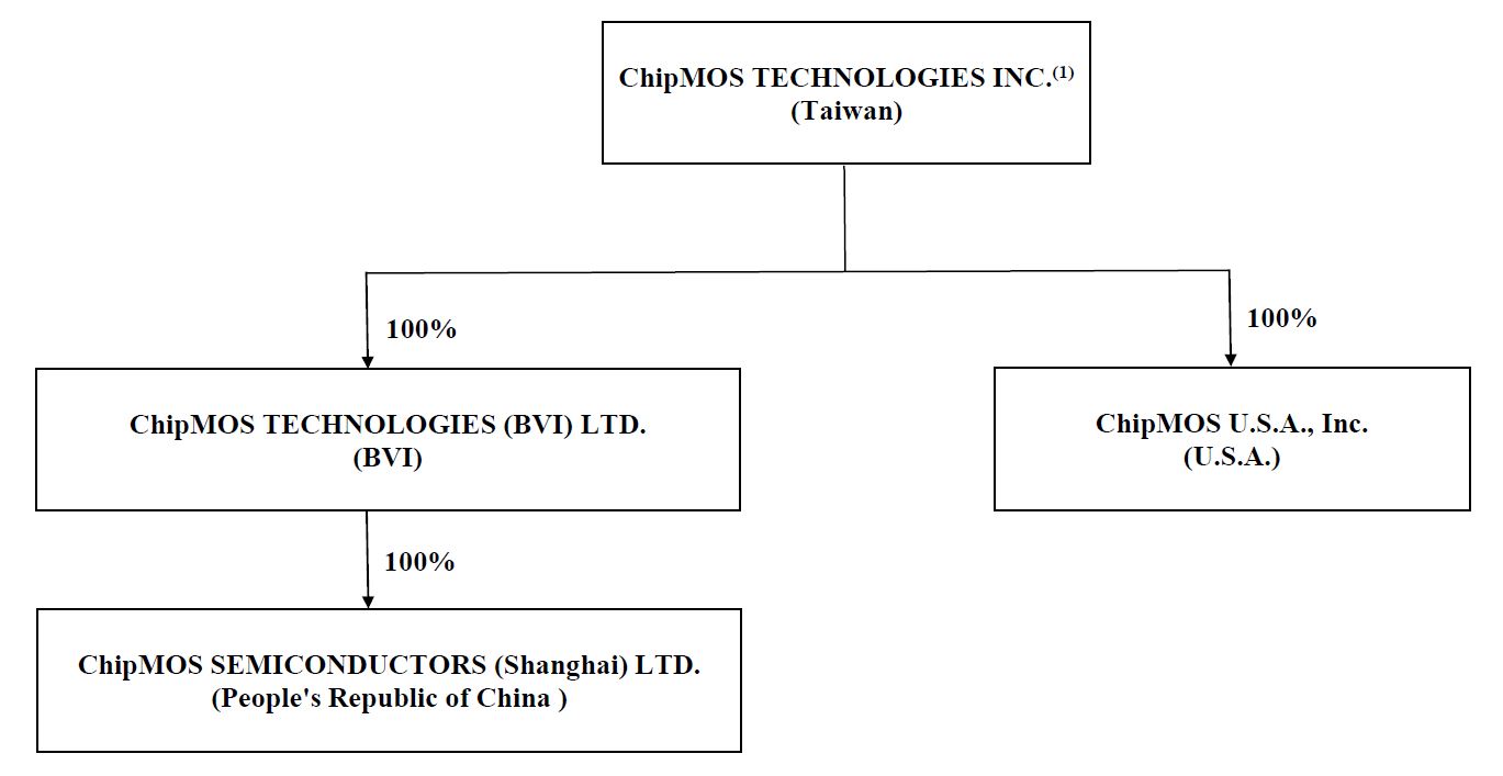
17
Note:
Agreements with Tsinghua Unigroup Ltd.
On November 30, 2016, the Equity Interest Transfer Agreements among ChipMOS BVI, a wholly-owned subsidiary of the Company, and some strategic investors which including Unigroup Guowei, a subsidiary of Tsinghua Unigroup, were executed. Pursuant to the Equity Interest Transfer Agreements, ChipMOS BVI would sell 54.98% equity interests of its wholly-owned subsidiary, Unimos Shanghai, to the strategic investors, and Unigroup Guowei would hold 48% equity interests of Unimos Shanghai, and the other strategic investors, including a limited partnership owned by Unimos Shanghai’s employees, would own approximately 6.98% equity interest of Unimos Shanghai. The transaction was completed in March 2017. Unimos Shanghai is no longer the subsidiary of the Company following the completion of equity interest transfer. Also pursuant to the agreement, ChipMOS BVI and the strategic investors agreed to further invest RMB 1,074 million into Unimos Shanghai. The further investment was completed in two tranches, one in July 2017 at RMB 687 million and one in February 2018 at RMB 387 million. On December 16, 2019, Unigroup Guowei and one of the strategic investor sold and transferred all equity interests of Unimos Shanghai to Yangtze Memory, which holds 50% equity interests of Unimos Shanghai after completed transaction. On May 11, 2020, one of the strategic investor sold and transferred all equity interests of Unimos Shanghai to Yangtze Memory Technologies Co., Ltd. (“Yangtze Memory”), which holds 50.94% equity interests of Unimos Shanghai after completed transaction. On July 24, 2023, Yangtze Memory sold and transferred all equity interests of Unimos Shanghai to Yangtze Memory Technologies Holding Co., Ltd., (“Yangtze Memory Holding”), which holds 50.94% equity interests of Unimos Shanghai after completed transaction.
Agreements with Suzhou Oriza PuHua ZhiXin Equity Investment Partnership (L.P.)
On December 21, 2023, the Company’s Board of Directors approved its wholly-owned subsidiary, ChipMOS BVI to sell its entire 45.0242% equity interests in Unimos Shanghai for a total sale price of RMB 979.3 million in cash. Under the proposed agreement, ChipMOS BVI will sell its entire remaining 45.0242% equity interests in Unimos Shanghai to Suzhou Oriza PuHua ZhiXin Equity Investment Partnership (L.P.) and other local Chinese investment management companies. The equity interest transfer is expected to be completed in the first half of 2024. For additional information on the transaction, see “Item 5. Operating and Financial Review and Prospects—Recent Acquisition”.
Our Principal Consolidated Subsidiaries
Below is a description of our principal consolidated subsidiaries:
ChipMOS TECHNOLOGIES (BVI) LTD., or formerly known as MODERN MIND TECHNOLOGY LIMITED ChipMOS BVI was incorporated in the British Virgin Islands in January 2002.
ChipMOS SEMICONDUCTORS (Shanghai) LTD. ChipMOS Shanghai was incorporated in Mainland China in March 2020, which is a wholly-owned subsidiary of ChipMOS BVI. It primarily engaged in providing marketing of semiconductors and electronic related produces, for its parent company and affiliates, throughout Mainland China.
ChipMOS U.S.A., Inc. ChipMOS USA was incorporated in the United States of America in October 1999. It is primarily engaged in providing marketing of semiconductors and electronic related produces, for its parent company and affiliates, throughout the United States of America. ChipMOS USA began generating revenue in 2001.
Industry Background
We provide a broad range of back-end assembly and testing services. Testing services include engineering test, wafer probing and final test of memory and logic/mixed-signal semiconductors. We also offer a broad selection of leadframe- and organic substrate-based package assembly services for memory and logic/mixed-signal semiconductors. In addition, we provide gold bumping, reel to reel assembly and testing services for LCD, OLED, automotive panel and other display panel driver semiconductors by employing COF and COG technologies.
18
Semiconductors tested and assembled by us are used in personal computers, graphics applications such as game consoles, communications equipment, mobile products, such as cellular handsets, tablets, consumer electronic products, automotive/industry and display applications such as display panels. In 2023, 20.6% of our revenue was derived from testing services for memory and logic/mixed-signal semiconductors, 21.7% from assembly services for memory and logic/mixed-signal semiconductors, 36.6% from Display panel driver semiconductor assembly and testing services and 21.1% from bumping services for semiconductors, respectively.
In additional, stable long-term demand and high margin are basic characters of automotive application. More semiconductor chips and display panel are consumed with the trend of popularization of automotive panels and Electric Vehicle (EV) could benefit our margin and increase our earnings.
Semiconductor Industry Trends
Growth in the semiconductor industry is largely driven by end-user demand for consumer electronics, communications equipment and computers, for which semiconductors are critical components. The overall semiconductor industry supply chain inventory level increases and end-demand rapidly decrease influenced by geopolitics and global inflationary pressures in the second half of 2022. These macro headwinds impacted end-demand since second half of 2022. In 2023, there are some ongoing fluctuations in our markets that impacted our end results.
Memory Semiconductor Market
The potential for memory market growth is linked to anticipated memory content increases in consumer electronics, data center, wireless base-station, PC and smartphone applications due to updated system requirements (such as 5G & wifi 6), increasing use of storage, graphics in gaming and other applications. The memory market is dominated by two segments-DRAM and flash memory. Potential growth in the DRAM and NAND Flash market is expected to be driven by continued growth in both the commodity and niche DRAM market, as well as growth opportunities in mobile DRAM as memory requirements significantly increase for mobile applications and storage requirement for data center application. Flash memory market potential growth is expected to be driven by increasing memory requirements for cellular handsets, digital cameras, digital audio/video, server, wireless base-station and other mobile applications, and new application demand of NOR flash for automotive/industry, OLED panel and touch with display driver integration (TDDI).
LCD, OLED, automotive panel and Other Display panel Driver Semiconductor Market
Display panels are used in applications such as desktop monitors, notebooks, tables, television sets, cellular handsets and digital cameras. The end-user demand for LCD, OLED, automotive panel and other display panel driver semiconductors tends to very over time. The soft demand of TVs impacted our utilization level of COF assembly. Regarding the small panel application, an integrated driver IC solution, TDDI, which became main stream of smart phone panel since 2021. OLED and automotive panel DDIC growth in the second half of 2022. Also, as more and more displays are installed in cars and EV, more driver IC grew for automotive application in 2023.
Logic/Mixed-Signal Semiconductor Market
The communications market is one of the main drivers of potential growth in the semiconductor industry. Logic/mixed-signal semiconductors, which are chips with analog functionality covering more than half of the chip area, are largely used in the communications market. The increasing use of digital technology in communications equipment requires chips with both digital and analog functionality for applications such as modems, network routers, switches, cable set-top boxes and cellular handsets. As the size and cost of cellular handsets and other communications-related devices have decreased, components have increased in complexity. Logic/mixed-signal semiconductors, such as LCD controller, power devices, fingerprint sensors and MEMS products, TV scaler and DVD controllers, are also used in consumer electronic products.
19
Overview of the Semiconductor Manufacturing Process
The manufacturing of semiconductors is a complex process that requires increasingly sophisticated engineering and manufacturing expertise. The manufacturing process may be broadly divided into the following stages:
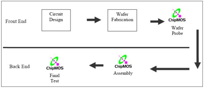
Process
|
Description
|
Circuit Design |
The design of a semiconductor is developed by laying out circuit patterns and interconnections. |
|
|
Wafer Fabrication |
Wafer fabrication begins with the generation of a photomask, a photographic negative onto which a circuit design pattern is etched or transferred by an electron beam or laser beam writer. Each completed wafer contains many fabricated chips, each known as a die. |
|
|
Wafer Probe |
Each individual die is then electrically tested, or probed, for defects. Dies that fail this test are discarded, or, in some cases, salvaged using laser repair. |
|
|
Assembly |
The assembly of semiconductors serves to protect the die, facilitates its integration into electronic systems and enables the dissipation of heat. The process begins with the dicing of the wafers into chips. Each die is affixed to a leadframe-based or organic substrate-based substrate. Then, electrical connections are formed, in many cases by connecting the terminals on the die to the inner leads of the package using fine metal wires. Finally, each chip is encapsulated for protection, usually in a molded epoxy enclosure. |
|
|
Final Test |
Assembled semiconductors are tested to ensure that the device meets performance specifications. Testing takes place on specialized equipment using software customized for each application. For memory semiconductors, this process also includes “burn-in” testing to screen out defective devices by applying very high temperatures and voltages onto the memory device. |
Outsourcing Trends in Semiconductor Manufacturing
Historically, integrated device manufacturers (“IDMs”), designed, manufactured, tested and assembled semiconductors primarily at their own facilities. In recent years, there has been a trend in the industry to outsource various segments of stages in the manufacturing process to reduce the high fixed costs resulting from the increasingly complex manufacturing process. Virtually every significant stage of the manufacturing process can be outsourced. The independent semiconductor manufacturing services market currently consists of wafer fabrication and probing services and semiconductor assembly and testing services. Most of the world’s major IDMs now use some independent semiconductor manufacturing services to maintain a strategic mix of internal and external manufacturing capacity. Many of these IDMs are continuously significantly reducing their investments in new semiconductor assembly and testing facilities.
20
The availability of technologically advanced independent semiconductor manufacturing services has also enabled the growth of “fabless” semiconductor companies that focus exclusively on semiconductor design and marketing and outsource their fabrication, assembly and testing requirements to independent companies.
We believe the outsourcing of semiconductor manufacturing services, and in particular of assembly and testing services, will increase for many reasons, including the following:
Significant Capital Expenditure Requirements. Driven by increasingly sophisticated technological requirements, wafer fabrication, assembly and testing processes have become highly complex, requiring substantial investment in specialized equipment and facilities and sophisticated engineering and manufacturing expertise. In addition, product life cycles have been shortened magnifying the need to continuously upgrade or replace manufacturing, assembly and testing equipment to accommodate new products. As a result, new investments in in-house fabrication, assembly and testing facilities are becoming less desirable for IDMs because of the high investment costs, as well as difficulties in achieving sufficient economies of scale and utilization rates to be competitive with the independent service providers. On the contrary, independent foundry, assembly and testing companies are able to realize the benefits of specialization and achieve economies of scale by providing services to a large customer base across a wide range of products. This enables them to reduce costs and shorten production cycles through high capacity utilization and process expertise.
Increasing Focus on Core Competencies. As the costs of semiconductor manufacturing facilities increase, semiconductor companies are expected to further outsource their wafer fabrication, assembly and testing requirements to focus their resources on core competencies, such as semiconductor design and marketing.
Time-to-Market Pressure. Increasingly short product life cycles have amplified time-to-market pressure for semiconductor companies, leading them to rely increasingly on independent companies as a key source for effective wafer fabrication, assembly and testing services.
Semiconductor Assembly and Testing Services Industry
Growth in the semiconductor assembly and testing services industry is driven by increased outsourcing of the various stages of the semiconductor manufacturing process by IDMs and fabless semiconductor companies.
The Semiconductor Industry and Conditions of Outsourcing in Taiwan and Mainland China
Taiwan is one of the world’s leading locations for outsourced semiconductor manufacturing. The semiconductor industry supply chain in Taiwan has developed such that the various stages of the semiconductor manufacturing process have been disaggregated, thus allowing for specialization. The disaggregation of the semiconductor manufacturing process in Taiwan permits these semiconductor manufacturing service providers to focus on particular parts of the production process, develop economies of scale, maintain higher capacity utilization rates and remain flexible in responding to customer needs by lowering time-to-market pressure faced by semiconductor companies. There are several leading service providers in Taiwan, each of which offers substantial capacity, high-quality manufacturing, leading semiconductor wafer fabrication, test, assembly and process technologies, and a full range of services. These service providers have access to an educated labor pool and a large number of engineers suitable for sophisticated manufacturing industries. As a result, many of the world’s leading semiconductor companies outsource some or all of their semiconductor manufacturing needs to Taiwan’s semiconductor manufacturing service providers and take advantage of the close proximity among facilities in the supply chain. In addition, companies located in Taiwan are very active in the design and manufacture of electronic systems, which has created significant local demand for semiconductor devices.
A few years ago, Mainland China had emerged as an attractive location for outsourced semiconductor manufacturing. Companies could take advantage of strongly supports by Mainland China government to accelerate the development of the semiconductor industry and a large domestic market. These factors had driven increased relocation of much of the electronics industry manufacturing and supply chain to Mainland China. But according to the economics uncertainty caused by the trade tensions and US semiconductor restrictions, the related investment risk in China is increasing. An increasing number of global electronic systems manufacturers and contract manufacturers are relocating or have relocated production facilities away from Mainland China.
Our Strategy
Our goal is to reinforce our position as a leading independent provider of semiconductor assembly and testing services, concentrating principally on memory, logic/mixed-signal and LCD, OLED, automotive panel and other display panel driver semiconductors. The principal components of our business strategy are set forth below.
21
Focus on Providing Our Services to Potential Growth Segments of the Semiconductor Industry.
We intend to continue our focus on developing and providing advanced assembly and testing services for potential growth segments of the semiconductor industry, such as memory, logic/mixed-signal, MEMS, LCD, OLED, automotive panel and other display panel driver semiconductors and bumping services. We believe that our investments in equipment and research and development in some of these areas allow us to offer a service differentiated from that of our competition. In order to benefit from the expected resumption of growth in these segments, we intend to continue to invest in capacity to meet the assembly and testing requirements of these key semiconductor market segments.
Continue to Invest in the Research and Development of Advanced Assembly and Testing Technologies.
Critical to our business growth is the continuation to expand our capabilities in testing and assembly and integrate wafer bumping and assembly core technologies to provide turn-key total solution service to our customers. We typically focus on advanced technologies that consist of greater potentials to generate higher margins. For example, we conducted new product introductions and on an on-going basis continue to expand our capabilities in fine-pitch wafer bumping, multi-chip package (“MCP”) and flip chip packaging. We have also introduced low cost metal composite bump (“MCB”) products based on our proprietary Copper plating technology to service display panel market and expand offerings to other business regions. We continue to maintain close working relationships with local and overseas research institutions and universities to keep abreast with leading edge technologies and broaden the scope of applications.
In 2023, we focus our research and development efforts in the following areas:
In 2023, we spent approximately 5.1% of our revenue on research and development. We will continue to invest our resources to recruit and retain experienced research and development personnel. As of February 29, 2024, our research and development team comprised 698 employees.
Build on Our Strong Presence in Taiwan and Strong Industrial Position Outside Taiwan.
We intend to build on our strong presence in key centers of semiconductor and electronics manufacturing to grow our business. Currently, most of our operations are in Taiwan, one of the world’s leading locations for outsourced semiconductor manufacturing. This presence provides us with several advantages. Firstly, our proximity to other semiconductor companies is attractive to customers who wish to outsource various stages of the semiconductor manufacturing process. Secondly, our proximity to many of our suppliers, customers and the end-users of our customers’ products enables us to be involved in the early stages of the semiconductor design process, enhances our ability to quickly respond to our customers’ changing requirements and shortens our customers’ time-to-market. Thirdly, we have access to an educated labor pool and a large number of engineers who are able to work closely with our customers and other providers of semiconductor manufacturing services.
Depending on customer’s demands, market conditions and other relevant considerations, we may from time to time look into other opportunities to expand our operations outside of Taiwan.
Expand Our Offering of Vertically Integrated Services.
We believe that one of our competitive strengths is our ability to provide vertically integrated services to our customers. Vertically integrated services consist of the integrated testing, assembly and direct shipment of semiconductors to end-users designated by our customers. Providing vertically integrated services enables us to shorten lead times for our customers. As time-to-market and cost increasingly become sources of competitive advantage for our customers, they increasingly value our ability to provide them with comprehensive back-end services.
22
We are able to offer vertically integrated services for a broad range of products, including memory, logic/mixed-signal and LCD, OLED, automotive panel and other display panel driver semiconductors. These services offerings include complementary technologies, products and services as well as additional capacity. We believe that these will continue to enhance our own development and expansion efforts into new and potential growth markets. We intend to establish new alliances with leading companies and, if suitable opportunities arise, engage in merger and acquisition activities that will further expand the services we can provide.
Focus on Increasing Sales through Long-Term Agreements with Key Customers as well as Business with Smaller Customers.
From time to time, we strategically agree to commit a portion of our assembly and testing capacity to certain of our customers. We intend to continue focus on increasing sales to key customers through long-term capacity agreements. The customers with which we entered long-term agreements include a reputable memory customer based in the U.S. See “—Customers” below for a more detailed discussion of these long-term agreements.
Global market and economic conditions have been unprecedented and challenging with tight credit conditions and recession in most major economies since 2008. In the fourth quarter of 2021, a long term 3-year capacity secure agreement with our customer about high end wafer test for OLED and other display panel driver demand was settled to reduce our investment risk. We also resumed our focus on our business with smaller customers or customers who do not place orders on a regular basis. We believe that the dual focused strategy will assist us to be better prepared for the current economic volatility and ensure maximum utilization rate of our capacity and help us to develop closer relationships with all types of our customers.
Principal Products and Services
The following table presents, for the periods shown, revenue by service segment as a percentage of our revenue.
|
|
Year ended December 31, |
||||
|
|
2021 |
|
2022 |
|
2023 |
Testing |
|
21.5% |
|
22.3% |
|
20.6% |
Assembly |
|
29.1% |
|
28.5% |
|
21.7% |
Display panel driver semiconductor assembly and testing |
|
30.0% |
|
31.0% |
|
36.6% |
Bumping |
|
19.4% |
|
18.2% |
|
21.1% |
Total revenue |
|
100.0% |
|
100.0% |
|
100.0% |
Memory and Logic/Mixed-Signal Semiconductors
Testing
We provide testing services for memory and logic/mixed-signal semiconductors:
Memory. We provide testing services for huge amount of varieties of memory semiconductors, such as SRAM, DRAM and Flash memory. To speed up the time-consuming process of memory product testing, we provide parallel test, which includes the completion of a tested wafer in one touchdown (up to 3,000 plus DUTs testing simultaneously). Wafer type includes Aluminum PAD, RDL PAD, Cu Pillar, WLCSP and prober test temperature between -55°~150° and provide 30MHz ~ 143 MHz test speed for DRAM product, 50MHz ~ 400 MHz test speed for FLASH product. The memory semiconductors we tested were applying primarily in desktop computers, laptop, tablet computers, handheld consumer electronic, devices and wireless communication devices.
Logic/Mixed-Signal. We conduct tests on a wide variety of logic/mixed-signal semiconductors, with lead counts ranging from the single digits to over 1024 and data rate of up to 16Gbps. The semiconductors we test include high-end audio/video codec, networking/communications, MCU, LCD related, MEMS related, DDR related and automotive electronics used for home entertainment/media center, personal computer applications, network/communication, mobile smart devices and cars. We also test a variety of application specific integrated circuits (“ASICs”), for applications such as FHD/UHD/8K LCD TV with AI functions, Smartphone, Tablet PC and Cars etc.
The following is a description of our pre-assembly testing services:
Engineering Testing. We provide engineering testing services, including software program development, electrical design validation, reliability and failure analysis.
23
Wafer Probing. Wafer probing is a processing stage proceeding to the assembly of semiconductors and which involves visual inspection and electrical testing to ensure the processed wafers meets our customers’ specifications. Tests are conducted using specialized equipment with software customized for each application in different temperature conditions ranging from -55 degrees Celsius to 150 degrees Celsius. Wafer probing employs sophisticated design and manufacturing technologies to connect the terminals of each chip for testing. Defect chips are marked on the surface or memorized in an electronic file, known as a mapping file, to the following facilitate subsequent process.
Laser Repairing. This is a unique process in testing operation for special SOC memory products. In laser repairing, specific poly or metal fuses are blown after wafer probing to enable a spare row or column of a memory unit in SOC the replacement of the defective memory cell.
After assembly, we perform the following testing services:
Burn-In Testing. This process screens out unreliable products using high temperature, high voltage and prolonged stresses environment to ensure that finished products will survive a long period of end-user service. This process is used only for memory products. This process needs customized Burn-In board.
Top Marking. By using laser marker, the marking content were according to our customers’ specification, including the logo, part number, date code and lot number.
Final Testing. Assembled semiconductors are tested to ensure that the devices meet performance specifications. Tests are conducted using specialized equipment with software customized for each application in different temperature conditions ranging from -55 degrees Celsius to 125 degrees Celsius.
Final Inspection and Packing. Final inspection involves visual or auto-inspection of the devices to check any bent leads, ball damage, inaccurate markings or other package defects. Packing involves dry packing, package-in-tray, package-in-tube and tape and reel. According to package level, Dry packing involves heating semiconductors in a tray at 125 degrees Celsius for about four to six hours to remove the moisture before the semiconductors are vacuum-sealed in an aluminum bag. Package-in-tube involves packing the semiconductors in anti-static tubes for shipment. Tape and reel pack involves transferring semiconductors from a tray or tube onto an anti-static embossed tape and rolling the tape onto a reel for shipment to customers.
Assembly
Our assembly services generally involve the following steps:
Wafer Lapping |
The wafers are ground to their required thickness. |
|
|
Die Saw |
Wafers are cut into individual dies, or chips, in preparation for the die-attach process. |
|
|
Die Attach |
Each individual die is attached to the leadframe or organic substrate. |
|
|
Wire Bonding |
Using gold or silver wires, to connect the I/O pads on the die to the inner lead of leadframe or substrate. |
|
|
Flip Chip Bonding |
Using solder bumps or Cu pillar bumps on die, to connect the leadframe or substrate pad via soldering reflow. |
|
|
Molding |
The die and wires are encapsulated to provide physical support and protection. |
|
|
Marking |
Each individual package is marked to provide product identification. |
|
|
24
Dejunking and Trimming |
Mold flash is removed from between the lead shoulders through dejunking, and the dambar is cut during the trimming process. |
|
|
Electrical Plating |
A solderable coating is added to the package leads to prevent oxidization and to keep solder wettability of the package leads. |
|
|
Ball Mount and Reflow |
Each electrode pad of the substrate is first printed with flux, after which solder balls are mounted, heated and attached to the electrode pad of the substrate through a reflow oven. |
|
|
Forming/Singulation |
Forming involves the proper configuration of the device packages leads, and singulation separates the packages from each other. |
We offer a broad range of package formats designed to provide our customers with a broad array of assembly services. The assembly services we offer customers are leadframe-based packages, which include thin small outline packages, and organic substrate-based packages, including fine-pitch BGA.
The differentiating characteristics of these packages include:
As new applications for semiconductor devices require smaller components, the size of packages has also decreased. In leading-edge packages, the size of the package is reduced to just slightly larger than the size of the individual chip itself in a process known as chip scale packaging.
As semiconductor devices increase in complexity, the number of electrical connections required also increases. Leadframe-based products have electrical connections from the semiconductor device to the electronic product through leads on the perimeter of the package. Organic substrate-based products have solder balls on the bottom of the package, which create the electrical connections with the product and can support large numbers of electrical connections.
Leadframe-Based Packages. These are generally considered the most widely used package category. Each package consists of a semiconductor chip encapsulated in a plastic molding compound with metal leads on the perimeter. This design has evolved from a design plugging the leads into holes on the circuit board to a design soldering the leads to the surface of the circuit board.
The following diagram presents the basic components of a standard leadframe-based package for memory semiconductors:
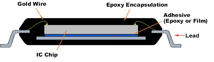
To address the market for miniaturization of portable electronic products, we are currently developing and will continue to develop increasingly smaller versions of leadframe-based packages to keep pace with continually shrinking semiconductor device sizes. Our advanced leadframe-based packages generally are thinner and smaller, have more leads and have advanced thermal and electrical characteristics when compared to traditional packages. As a result of our continual product development, we offer leadframe-based packages with a wide range of lead counts and sizes to satisfy our customers’ requirements.
The following table presents our principal leadframe-based packages, including the number of leads in each package, commonly known as lead-count, a description of each package and the end-user applications of each package.
25
Package
|
Lead-
|
Description
|
End-User Applications
|
Thin Small Outline Package I (TSOP I) |
48-56 |
Designed for high volume production of low lead-count memory devices, including flash memory, SRAM and MROM |
Notebooks, personal computers, still and video cameras and standard connections for peripherals for computers |
|
|
|
|
Thin Small Outline Package II (TSOP II) |
44-86 |
Designed for memory devices, including flash memory, SRAM, SDRAM and DDR DRAM |
Disk drives, recordable optical disk drives, audio and video products, consumer electronics, communication products |
Quad Flat No Lead (QFN) |
8-132 |
Thermal enhanced quad flat no lead package providing small footprint (chip scale), light weight with good thermal and electrical performance |
Wireless communication products, notebooks, PDAs, consumer electronics |
|
|
|
|
Low-Profile Quad Flat Package (LQFP) |
48 |
Low-profile and light weight package designed for ASICs, digital signal processors, microprocessors/ controllers, graphics processors, gate arrays, SSRAM, SDRAM, personal computer chipsets and mixed-signal devices |
Wireless communication products, notebooks, digital cameras, cordless/radio frequency devices |
|
|
|
|
Small Outline Package (SOP) |
8 |
Designed for low lead-count memory and logic semiconductors, including SRAM and micro-controller units |
Personal computers, consumer electronics, audio and video products, communication products |
|
|
|
|
Multi-Chip Package (TSOP) |
44-86 |
Our patented design for memory devices, including flash memory, SRAM, DRAM, SDRAM and DDR DRAM |
Notebooks, personal computers, disk drives, audio and video products, consumer products, communication products |
|
|
|
|
Flip Chip Quad Flat No Lead (FCQFN) |
6-35 |
Thermal enhanced quad flat no lead package providing small footprint (chip scale), light weight with good thermal and electrical performance Flip chip process is designed for better electrical performance compared to wire bonding process |
Wireless communication products, notebooks, PDAs, consumer electronics |
Organic Substrate-based Packages. As the number of leads surrounding a traditional leadframe-based package increases, the leads must be placed closer together to reduce the size of the package. The close proximity of one lead to another can create electrical shorting problems and requires the development of increasingly sophisticated and expensive techniques to accommodate the high number of leads on the circuit boards.
The BGA format solves this problem by effectively creating external terminals on the bottom of the package in the form of small bumps or balls. These balls are evenly distributed across the entire bottom surface of the package, allowing greater pitch between the individual terminals. The ball grid array configuration enables high-pin count devices to be manufactured less expensively with less delicate handling at installation.
Our organic substrate-based packages employ a fine-pitch BGA design, which uses a plastic or tape laminate rather than a leadframe and places the electrical connections, or leads, on the bottom of the package rather than around the perimeter. The fine-pitch BGA format was developed to address the need for the smaller footprints required by advanced memory devices. Benefits of ball grid array assembly over leadframe-based assembly include:
26
The following diagram presents the basic component parts of a fine-pitch BGA package:
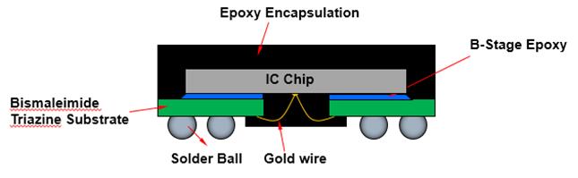
The following table presents the ball-count, description and end-user applications of organic substrate-based packages we currently assemble:
|
|
|
|
Package
|
Connections
|
Description
|
End-User Applications
|
Mini BGA |
24-400 |
Low-cost and space-saving assembly designed for low input/output count, suitable for semiconductors that require a smaller package size than standard BGA |
Memory, analog, flash memory, ASICs, radio frequency devices, personal digital assistants, cellular handsets, communication products, notebooks, wireless systems |
|
|
|
|
Fine-Pitch BGA |
54-126 |
Our patented design for DRAM products that require high performance and chip scale package (CSP) |
Notebooks, cellular handsets, global positioning systems, personal digital assistants, wireless systems |
|
|
|
|
Very Thin Fine-Pitch BGA |
48-176 |
Similar structure of Mini BGA package with thinner and finer ball pitch that is designed for use in a wide variety of applications requiring small size, high reliability and low unit cost |
Handheld devices, notebooks, disk drives, wireless and mobile communication products |
|
|
|
|
Land Grid Array (LGA) |
8-52 |
Thinner and lighter assembly designed essential to standard BGA without solder balls, suitable for applications that require high electrical performance |
Disk drives, memory controllers, wireless, mobile communication products |
|
|
|
|
Multi-Chip BGA |
48-153 |
Designed for assembly of two or more memory chips (to increase memory density) or combinations of memory and logic chips in one BGA package |
Notebooks, digital cameras, personal digital assistants, global positioning systems, sub-notebooks, board processors, wireless systems |
|
|
|
|
Stacked-Chip BGA |
24-345 |
Designed for assembly of two or more memory chips or logic and memory chips in one CSP, reducing the space required for memory chips |
Cellular handsets, digital cameras, personal digital assistants, wireless systems, notebooks, global positioning systems |
|
|
|
|
FC Chip-scale Package (FC CSP) |
16-872 |
Better IC protection and solder joint reliability compared to direct chip attach (DCA) and chip on board (COB) |
Memory, logic, microprocessor, application processor (AP), baseband (BB), solid state device, radio frequency (RF) |
|
|
|
|
Multi-Chip Hybrid Package (FC+WB) |
153-345 |
Designed for assembly of two or more memory chips or combinations of memory and logic chips in one BGA package with both of flip chip and wire bonding |
Embedded Multi Media Card (eMMC), Universal Flash Storage (UFS), and BGA SSD |
|
|
|
|
27
|
|
|
|
Package
|
Connections
|
Description
|
End-User Applications
|
Chip on Wafer (CoW) |
5-30 |
Integrated two different functional chips to a closer form into a compact package. Low-cost solution compared to through-silicon via (TSV) |
Integrated MEMS |
|
|
|
|
Land Grid Array (LGA) for FPS (Finger Print Sensor) |
20-52 |
Very thin clearance (50um) between chip & compound hard color coating with scratch resistance for protection and appearance matching of mobile devices |
Security protection for mobile devices, home, notebooks, etc. |
|
|
|
|
Wafer Level Chip Scale Package (WLCSP) |
6-125 |
WLCSP package size is almost the same as die size. Simple assembly process flow, low cost. Small package suitable to apply on hand-held 3C electronic products |
Electronic Compass, audio converter, nor flash product, power control, sensor magnetometer, MEMS magnetometer, CMOS Image Sensor controller, Laser diode driver, power manager IC (PMIC) |
Wafer Level CSP
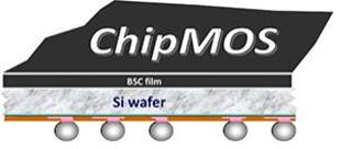
Wafer-level CSP (WLCSP) is the technology of packaging an integrated circuit at wafer level. WLCSP is essentially a true chip scale package (CSP) technology, since the resulting package is practically of the same size as the die. WLCSP has the ability to enable true integration of wafer fab, packaging, test, and burn-in at wafer level in order to streamline the manufacturing process undergone by a device start from silicon wafer to customer shipment.
Most other kinds of packaging do wafer dicing first, and then puts the individual die in a plastic package and attaches the solder bumps. WLCSP involves the RDL, wafer solder bumping, while still in the wafer, and then wafer dicing. Benefits of WLCSP compare to general CSP package assembly include:
Package
|
Connections
|
Description
|
End-User Applications
|
WLCSP |
4-96 |
Very small package size (identical to die size), suitable for the low pin count and require the small package size application |
Memory, ASICs, PMIC, MEMS devices, controllers, for mobile phones, tablets, ultra book computers and wearable products |
28
FC CSP
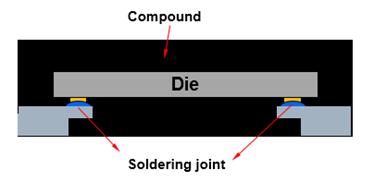
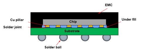
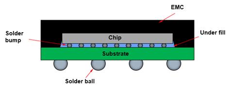
FC Chip Scale Package (FC CSP) construction utilizes the flip chip bumping (with solder bump or Cu pillar bump) interconnection technology to replace the standard wire-bond interconnect. It allows for a smaller form factor due to wire loop reduction and area array bumping. FC CSP includes the substrate or leadframe type solution making an attractive option for advanced CSP application when electrical performance is a critical factor.
Package
|
Connections
|
Description
|
End-User Applications
|
FC CSP |
8-1288 |
Superior electrical performance, smaller form factor |
Power devices, RF, High speed Logic devices, wireless, memory or portable applications |
29
Display Driver Semiconductors and Gold MCB Bumping
We also offer assembly and testing services for display driver semiconductors. We employ COF and COG technologies for testing and assembling display driver semiconductors. In addition, we offer gold bumping and metal composite bump services to our customers.
Note: Copper pillar service only for Max size: 9.8mmx8.2mm & pillar Account: 3401
Chip-on-Film (COF) Technology
COF technology provides several additional advantages. For example, COF is able to meet the size, weight and higher resolution requirements in electronic products, such as display panels. This is because of its structural design, including an adhesive-free two-layer tape that is highly flexible, bending strength and its capacity to receive finer patterning pitch.
COF package has been using for large-size and high-resolution panel display, especially on TFT-LCD and OLED TV set and NB as well. In recent years, there has been an observable trend with which the average inner lead pitch of COF package went down to 23um with more than 80% of market demand. High thermal dissipation packaging technology is available for mass production. And dual IC with high thermal dissipation COF packaging technology is ready for 8K TV market. 18um/16um inner lead pitch 2-metal layer COF package is in development for coming AR/VR gear requirement. And we can test display driver semiconductors with frequency up to 6.5Gbps to fulfill high speed data rate requirement. For automotive application, low temperature COF package testing technology is developed.
The following diagram presents the basic components of 1-metal layer COF and 2-metal layer COF:

The COF process involves the following steps:
Chip Probing |
Screen out the defect chips which fail to meet the device spec. |
|
|
Wafer Lapping/Polish
Laser Marking
Laser Grooving |
Wafers are grounded or with polish to their required thickness.
A laser mark is applied on IC backside in wafer form to provide product traceability.
Application in wafer within Low-K material to reduce chipping of chips during dicing process. |
|
|
Die Saw |
Wafers are cut into individual dies, or chips, in preparation for inner lead bonding process. |
|
|
Inner Lead Bonding |
An inner lead bonding machine connects the chip to the printed circuit tape. |
|
|
Potting |
An underfill process to fill resin to protect the inner lead and chip. |
|
|
Potting Cure |
The potting cure process matures the resin used during the potting oven with high temperatures. |
|
|
Marking |
A laser marker is used to provide product identification. |
|
|
Final Testing |
To verify device spec. within electrical testing after assembly process. |
|
|
Taping |
To attach heat sink/spreader or stiffener material onto COF package. |
|
|
Inspection and Packing |
Each individual die with tape is visually or auto inspected for defects. The dies are packed within a reel into an aluminum bag after completion of the inspection process. |
30
Chip-on-Glass (COG) Technology
COG technology is an electronic assembly technology that is used in assembling display driver semiconductors including TV/monitor, mobile and wearable products. Compared to the traditional bonding process for COF, the new COG technology requires lower bonding temperature. In addition, the COG technology reduces assembly cost as it does not use tapes for interconnection between the LCD, OLED panel and the printed circuit board. The major application of COG products is on TFT-LCD and AMOLED display of smart phone and automotive market, it integrates source, gate driver of display driver IC (DDIC) and touch or timing Controller IC into one chip, so the output channel is higher than COF products. For the market trend of thinner smartphone, 150um in IC thickness is released for mass production and much thinner IC thickness is in development.
The COG assembly process involves the following steps:
Chip Probing |
To screen out the defect chips which fail to meet the device spec. |
|
|
Wafer Lapping/Polish |
Wafers are ground or with polished to their required thickness. |
|
|
Laser Marking |
A laser mark is applied on IC backside in wafer form to provide product traceability. |
|
|
Laser Grooving |
Application in wafer within Low-K material to reduce chipping of chips during dicing process. |
|
|
Die Saw |
Wafers are cut into individual dies, or chips, in preparation for the pick and place process. |
|
|
Auto Optical Inspection |
Process of wafer inspection is detecting defect to separate chips at pick and place station. |
|
|
Pick and Place |
Each individual die is picked and placed into a chip tray. |
|
|
Inspection and Packing |
Each individual die in a tray is visually or auto-inspected for defects. The dies are packed within a tray into an aluminum bag after completion of the inspection process. |
Bumping
We also offer bumping services to our customers.
Based on the major product portfolio (judged by internal metal composition), we provide:
Gold bumping technology, which is in high demand for LCD driver ICs. In 2021, we increased gold bumping wafer shipments resulting from demand for of high refresh rate panel, 5G mobile, gaming monitor, 8K display and automotive infotainment applications. In 2022, ChipMOS also developed VR/AR wearable devices for some new application opportunities, including metaverse. Meanwhile, medical, automotive and integration TDDI products are still our main business goal. In 2023, gold bumping development momentum will be emphasized on new products from OLED display penetration rate of smartphone, another focused business is that automotive category products continue to expand. In 2024, Display driver ICs conventional gold plating technology is matured and face severe competitiveness pressure from competitors. The major cost among all process is gold, extremely high cost structure ratio and gold price is no sign to downward trend. It’s good opportunity to deploy Ag-Alloys bumps technology. We aim to introduce silver bump to the market.
As high speed, high performance and high accuracy requirement, many electronic devices need the capability of transferring higher current. By using Re-distribution layer (RDL) technology which can relocate to the PKG wire bonding position where necessary. ChipMOS can provide several electroplating metal thickness based on customer design request, including 2P1M, 2P2M and 3P2M structures. The min. Line/space of RDL could be 5/5um that makes integration of MCP and SIP achievable. For electric property requirement, thicker thickness structure is also available, that enables total thickness to 25um. In 2024, we will deliver new Silver-Alloys electroplating RDL technology which transmits signals and performs better electrical property. We aim to replace conventional Cu/Ni/Au process with several advantages due to Silver is characterized with highly conductive, stretchable properties. Main advantages: The highest electrical conductivity, the highest thermal conductivity and proven good solderability/metal connector in semiconductor field.
31
We believe that consumer electronics are driving the application growth of these processes. From small wearable gadgets, NOR flash applications, power devices to emerging AIoT/AI development are all included. We expanded our bumping factory line capacity toward the consumer market and we expect this to continue to deliver good performance. Through 12” WLCSP process for NOR flash to provide a thinner and smallest chip size for TWS (True Wireless Stereo) application is a success case recently. Now, Copper pillar and flip chip solution is another packaging solution for this application. Fine pitch Copper pillar is an effective way to increase interconnection densities. The typical Copper pillar height is 50~70 um, further development is micro bump, which advances Copper pillar pitch and size to 45/25 um. Copper pillar size and height. Copper pillar also offers advantages with respect to better electrical and thermal conductivity, as well as increasing electromigration resistance and current carrying capability. We are developing taller bump height up to 110um for power devices and adding it into mass production portfolio in the third quarter of 2023. In 2024, the structure portfolio will involve 3P3M WLCSP, 1P2M metal first, 1P2M PI first with followed 2 layer metals. As for new material, we deliver new solder ball SACQ and high curable polymer HD4100 development for new WLCSP projects. Also implement HD4100 to NPI for many clients assignment. In WLCSP backend, we take efforts to non-backside coating requirement for customer to cost reduction.
Other Services
Drop Shipment
We offer drop shipment of semiconductors directly to end-users designated by our customers. We provide drop shipment services, including assembly in customer-approved and branded boxes, to a majority of our assembly and testing customers. Since drop shipment eliminates the additional step of inspection by the customer prior to shipment to end-users, quality of service is a key to successful drop shipment service. We believe that our ability to successfully execute our full range of services, including drop shipment services, is an important factor in maintaining existing customers as well as attracting new customers.
Software Development, Conversion and Optimization Program
We work closely with our customers to provide sophisticated software engineering services, including test program development, conversion and optimization, and related hardware design. Generally, testing requires customized testing software and related hardware to be developed for each particular product. Software is often initially provided by the customer and then converted by us at our facilities for use on one or more of our testing machines and contains varying functionality depending on the specified testing procedures. Once a conversion test program has been developed, we perform correlation and trial tests on the semiconductors.
Customer feedback on the test results enables us to adjust the conversion test programs prior to actual testing. We also typically assist our customers in collecting and analyzing the test results and recommends engineering solutions to improve their design and production process.
Customers
We believe that the following factors have been, and will continue to be, important factors in attracting and retaining customers:
32
The number of our customers as of February 28 of 2022, 2023 and February 29, 2024, respectively, was 72, 73 and 67. Our top 15 customers in terms of revenue in 2023 were (in alphabetical order):
Asahi Kasei Microdevices Corporation
Chipone Technology (Beijing) Co., Ltd.
Cypress Semiconductor Corporation
Elite Semiconductor Microelectronics Technology Inc.
GigaDevice Semiconductor (HK) Limited
Himax Technologies, Inc.
ILI Technology Corporation
Integrated Circuit Solution Inc.
Macronix International Co., Ltd.
Micron Technology, Inc.
Novatek Microelectronics Corp.
OmniVision Touch and Display Technologies Pte. Ltd.
Phison Electronics Corp.
Raydium Semiconductor Corporation
Winbond Electronics Corporation
In 2021, our top three customers accounted for approximately 21%, 10% and 9% of our revenue, respectively. In 2022, our top three customers accounted for approximately 20%, 10% and 9% of our revenue, respectively. In 2023, our top three customers accounted for approximately 25%, 13% and 9% of our revenue, respectively.
The majorities of our customers purchase our services through purchase orders and provide us three-month non-binding rolling forecasts on a monthly basis. The price for our services is typically agreed upon at the time when a purchase order is placed.
The following table sets forth, for the periods indicated, the percentage breakdown of our revenue, categorized by geographic region based on the jurisdiction in which each customer is headquartered.
|
|
Year ended December 31, |
||||
|
|
2021 |
|
2022 |
|
2023 |
Taiwan |
|
79% |
|
79% |
|
81% |
Japan |
|
6% |
|
9% |
|
6% |
PRC |
|
7% |
|
8% |
|
8% |
Singapore |
|
6% |
|
2% |
|
3% |
Others |
|
2% |
|
2% |
|
2% |
Total |
|
100% |
|
100% |
|
100% |
Qualification and Correlation by Customers
Our customers generally require that our facilities undergo a stringent “qualification” process during which the customer evaluates our operations, production processes and product reliability, including engineering, delivery control and testing capabilities. The qualification process typically takes up to eight weeks, or longer, depending on the requirements of the customer. For test qualification, after we have been qualified by a customer and before the customer delivers semiconductors to us for testing in volume, a process known as “correlation” is undertaken. During the correlation process, the customer provides us with test criteria; information regarding process flow and sample semiconductors to be tested and either provides us with the test program or requests that we develop a new or conversion program. In some cases, the customer also provides us with a data log of results of any testing of the semiconductor that the customer may have conducted previously. The correlation process typically takes up to two weeks, but can take longer depending on the requirements of the customer.
Sales and Marketing
We maintain sales and marketing offices in Taiwan, the United States and Mainland China. Our sales and marketing strategy is to focus on memory semiconductors in Taiwan, Japan, Singapore, Korea and the United States, logic/mixed-signal semiconductors in Taiwan, Japan and the United States, LCD, OLED, automotive panel and other display panel driver semiconductors in Japan, Korea, Taiwan, Hong Kong and Mainland China. As of February 29, 2024, our sales and marketing efforts were primarily carried out by teams of sales professionals, application engineers and technicians, totaling 32 staff members. Each of these teams focuses on specific customers and/or geographic regions. As part of our emphasis on customer service, these teams:
33
We conduct marketing research through our in-house customer service personnel and through our relationships with our customers and suppliers to keep abreast of market trends and developments. Furthermore, we do product and system bench marking analysis to understand the application and assembly technology evolution, such as analysis on mobile handsets and Tablet, PC, wearable products. In addition, we regularly collect data from different segments of the semiconductor industry and, when possible, we work closely with our customers to design and develop assembly and testing services for their new products. Sale will cowork with internal technology expert to work closely with our customers as project kick off. We provide full turnkey service (from design-in stage/design for bumping and assembly/design for testing services) to achieve design for mass production for new products. These “co-development” or “sponsorship” projects can be critical when customers seek large-scale, early market entry with a significant new product.
Research and Development
To maintain our competitive edge for continued business growth, we continue our focus of our investment in new technology research and development. In 2021, 2022 and 2023, we spent approximately NT$1,139 million, or 4.2%, NT$1,159 million, or 4.9% and NT$1,093 million (US$36 million), or 5.1%, respectively, of our revenue on research and development.
Our research and development efforts have been focused primarily on new technology instruction, improving efficiency and production yields of our testing, assembly and bumping services. From time to time, we jointly develop new technologies with local and international equipment and material manufacturing company to enhance the competitiveness. In testing area, our research and development efforts focused particularly on high speed probing, fine pitch probing capability and wafer level burn-in technology. Our projects include:
In assembly and bumping areas, our research and development efforts were directed to:
34
For new product and product enhancement work in 2017, our work concentrates on three key development programs: 3D WLCSP, biometric sensor package solutions, and flip chip technology. In the bumping area, we completed customer qualification of 300mm wafer Au bumping process in 2012 and started volume production in the fourth quarter of 2012. Development of Cu plating enables the entry of WLCSP, RDL and flip chip market and Cu RDL applied on DRAM wafer for SiP product is qualified in 2016. Turnkey services of WLCSP and flip chip QFN have been implemented for mass production in 2013 based on the successful technology developments. In 2012, we also initiated both 200mm and 300mm Cu pillar bumping engineering work and, related packaging technologies are being developed for mixed-signal and memory products in 2013. It is also qualified on power management IC product in 2016. According wearable device trend, we miniature fine-pitch Cu RDL process for WLCSP and RDL products, we shrink ball size with ball mount technology and combine thinner wafer grinded thickness to achieve thin WLCSP structure in 2020 which used in Auto Focus, OIS (Optical Image Stabilization) system and Hall motor sensor. By integrating WLCSP bumping, copper pillar bumping and flip chip assembly capability, an integrated WLCSP (CoW or 3D WLCSP) is developing in 2015, and qualified the structure and process verification in 2016. We adopt FC Chip Scale Package to implement in USB4/DP2.0 Re-Driver, PCIe 5.0 Re-Driver Product in 2021. Meanwhile, fingerprint sensor (FPS) packaging solution by LGA was also developed for smartphone demand in 2015. More and more integrated function of DDIC, TDDI and FPS, is requested for smartphone application, therefore 2-metal layers COF solution and COF SMT are developed to provide the package solution since 2019. Moreover, the improved OLED panel yield rate has also increased its adoption in smartphones, leading to diverse applications such as in-display fingerprint sensors.
Since 2013, in-process engineering advancement allowed us to extend our wirebond technology to service MEMS products. To further achieve cost reduction, alloy wire and 0.6 mil Au wirebond processes were also developed. In 2018, we continued to work on the expansion of multi-chip NAND packages offerings, and 12” fine pitch COF assembly capability. Capability of handling miniature molded packages has been extended to 1x1 mm size and various improvements will also be made in production equipment to enhance throughput and efficiency. In 2019, we launched SDBG technology to implement multi-chip assembly and module of flash products for NAND Flash applications for SSD and eMMC applications.
As of February 29, 2024 we employed 698 employees in our research and development activities. In addition, other management and operational personnel are also involved in research and development activities but are not separately identified as research and development professionals.
We maintain laboratory facilities capable for materials and electrical characterizations to support production and new product development. Computer simulation is used to validate both mechanical and electrical models in comparison to measurement results. Enhancement of Shadow Moiré and Micro Moiré equipment was carried out to support MCP and flip chip package warpage and residue stress characterization. We also setup up mold flow simulation capability to predict assembly risk. In Advanced Packaging Lab, rheology measurement capability and high frequency electric simulation capability were established, aimed at expanding capability for material selection and inspection to support flip chip introduction and various resin characterizations. For customer application request, we enhance our thermal simulation capability in 2022. An analytical laboratory has been built out in our bumping line providing timely support to manufacturing operations.
Quality Control
We believe that our reputation for high quality and reliable services have been an important factor in attracting and retaining leading international semiconductor companies as customers for our assembly and testing services. We are committed to delivering semiconductors that meet or exceed our customers’ specifications on time and at a competitive cost. We maintain quality control staff at each of our facilities.
35
As of February 29, 2024, we employed 51 personnel for our quality control activities. Our quality control staff typically includes engineers, technicians and other employees who monitor assembly and test processes in order to ensure high quality. We employ quality control procedures in the following critical areas:
All of our facilities have obtained ISO 26262 road vehicles-functional safety system certification in December 2019 and obtained IATF 16949 quality system certification in December 2017. In addition, our facilities in Hsinchu and Tainan have been ISO 9002 certified in September 1997 and December 1998, respectively, and recertified with ISO 9001 for substantial revision since 2015.
IATF 16949 certification system seeks to integrate quality management standards into the operation of a company and emphasizes the supervision and measurement of process and performance. An ISO 9001 certification is required by many countries for sales of industrial products.
In addition to the quality management system, we also earned the 1998 QC Group Award from The Chinese Society of Quality, which is equivalent to the similar award from the American Society of Quality and certified ISO17025 in 2000. In 2003, ChipMOS passed SONY Green Partner (Tier 2) certification through its ProMOS channel, and in 2009, ChipMOS obtained SONY Green Partner (Tier 1) certification due to its direct business relationship with SONY. The Sony certificates will continue to be maintained uninterrupted until now. Our laboratories have also been awarded Chinese National Laboratory accreditation under the categories of reliability test, electricity and temperature calibration.
Our assembly and testing operations are carried out in clean rooms where air purity, temperature and humidity are controlled. To ensure the stability and integrity of our operations, we maintain clean rooms at our facilities that meet U.S. federal 209E class 100, 1,000, 10,000 and 100,000 standards. A class 1,000 clean room means a room containing less than 1,000 particles of contaminants per cubic foot.
We have established manufacturing quality control systems which are designed to maintain reliability and high production yields at our facilities. We employ the most advanced equipment for manufacturing quality and reliability control, including:
In addition, to enhance our performance and our research and development capabilities, we also installed a series of high-cost equipment, such as temperature humidity bias testers, low temperature storage-life testers and highly accelerated stress testers. We believe that many of our competitors do not own this equipment.
As a result of our ongoing focus on quality, in 2023, we achieved monthly assembly yields of an average of 99.93% for our memory and logic/mixed-signal assembly packages, 99.98% for our COF packages, 99.96% for our COG packages and 99.96% for our bumping products (including gold bump, RDL and WLCSP). The assembly yield, which is the industry standard for measuring production yield, is equal to the number of integrated circuit packages that are shipped back to customers divided by the number of individual integrated circuits that are attached to lead frames or organic substrate.
Raw Materials
Semiconductor testing requires minimal raw materials. Substantially all of the raw materials used in our memory and logic/mixed-signal semiconductor assembly processes are interconnect materials such as leadframes, organic substrates, gold wire and molding compound. Raw materials used in the LCD, OLED, automotive panel and other display panel driver semiconductor assembly and testing process include gold, carrier tape, resin, spacer tape, plastic reel, aluminum bags, and inner and outer boxes. Cost of raw materials represented 20%, 19% and 19% of our revenue in 2021, 2022 and 2023, respectively.
36
We do not maintain large inventories of leadframes, organic substrates, gold wire or molding compound, but generally maintain sufficient stock of each principal raw material for approximately two to three month’s production based on blanket orders and rolling forecasts of near-term requirements received from customers. Shortages in the supply of materials experienced by the semiconductor industry have in the past resulted in price adjustments. Our principal raw material supplies have not been impacted by the subcontractor production line shut down caused by COVID-19. See “Item 3. Key Information—Risk Factors—Risks Relating to Our Business—If we are unable to obtain raw materials and other necessary inputs from our suppliers in a timely and cost-effective manner, our production schedules would be delayed and we may lose customers and growth opportunities and become less profitable” for a discussion of the risks associated with our raw materials purchasing methods. For example, with the exception of aluminum bags and inner and outer boxes, which we acquire from local sources, the raw materials used in our COF process and for modules are obtained from a limited number of Japanese suppliers.
Competition
The independent assembly and testing markets are very competitive. Our competitors include large IDMs with in-house testing and assembly capabilities and other independent semiconductor assembly and testing companies, especially those offering vertically integrated assembly and testing services, such as Advanced Semiconductor Engineering Inc., Amkor Technology, Inc., Chipbond Technology Corporation, King Yuan Electronics Co., Ltd., Powertech Technology Inc., Jiangsu Changjiang Electronics Technology Co., Ltd. and United Test and Assembly Center Ltd. We believe that the principal measures of competitiveness in the independent semiconductor testing industry are:
In assembly services, we compete primarily on the basis of:
IDMs that use our services continually evaluate our performance against their own in-house assembly and testing capabilities. These IDMs may have access to more advanced technologies and greater financial and other resources than we do. We believe, however, that we can offer greater efficiency and lower costs while maintaining an equivalent or higher level of quality for three reasons:
Intellectual Property
As of February 29, 2024, we held 296 patents in Taiwan,94 patents in the United States, 160 patents in Mainland China, 1 patent in the United Kingdom and 2 patents in Korea and Japan, respectively, relating to various semiconductor assembly and testing technologies. These patents will expire at various dates through to 2042. As of February 29, 2024, we also had a total of 28 pending patent applications in Taiwan, and 73 in Mainland China. In addition, we have registered “ChipMOS” and its logo as trademarks in Taiwan, the United States, Mainland China, Singapore, Hong Kong, Korea, Japan, the United Kingdom and the European Community.
37
We expect to continue to file patent applications where appropriate to protect our proprietary technologies. We may need to enforce our patents or other intellectual property rights or to defend ourselves against claimed infringement of the rights of others through litigation, which could result in substantial costs and a diversion of our resources. See “Item 3. Key Information—Risk Factors—Risks Relating to Our Business—Disputes over intellectual property rights could be costly, deprive us of technologies necessary for us to stay competitive, render us unable to provide some of our services and reduce our opportunities to generate revenue”.
Government Regulations
As discussed above under “—Intellectual Property”, governmental regulation of our intellectual property may materially affect our business. The failure to protect our property rights would deprive us of our ability to stay competitive in the semiconductor industry. Our intellectual property rights are protected by the relevant patent and intellectual property agencies of the European Community, the United Kingdom, the United States, Mainland China, Singapore, Hong Kong, Korea, Japan and Taiwan.
Environmental and Climate Change Matters
Semiconductor testing does not generate significant pollutants. The semiconductor assembly and gold bumping process generate stationary acid, alkali and VOC pollutions, principally at the plating and etching stages. Water waste is produced when silicon wafers are ground thinner, diced into chips with the aid of diamond saws and cleaned with running water. In addition, excess materials, either on leadframes or molding process, are removed from assembled semiconductors in the trimming and de-junking processes, respectively. We have various treatment equipment for wastewater and air pollutants at our assembly and bumping facilities. Since 2001, we have adopted certain environmental friendly production management systems, and have implemented certain measures intended to bring our all processes in compliance with the Restriction of Hazardous Substances Directive/EC issued by the European Union and our customers. We believe that we have adequate and effective environmental protection measures that are consistent with semiconductor industry practices in Taiwan. In addition, we believe we are in compliance in all material respects with current environmental laws and regulations applicable to our operations and facilities.
All of our facilities in Taiwan have been certified as meeting the ISO 14001 environmental standards of the International Organization for Standardization, and all of our facilities in Taiwan have been certified as meeting the ISO 45001 standards of the International Organization for Standardization. Our facilities at Hsinchu Science Park, Chupei, Hukou, Hsinchu Industrial Park and Southern Taiwan Science Park have won numerous awards including “Green Factory Label” from 2013 to 2023, “Enterprises Environmental Protection Gold Grade Award” in 2018 and 2019, “Occupational Safety and Health Excellent Award” in 2016, 2017, 2021, 2022 and 2023, “Green Building Label” in 2014 and 2017 up to now. We are also certified the “Health Promotion Awards” from 2012 to 2024. We continue to encourage our employees to participate in community environmental campaigns and better environmental friendly practices.
We will continue to enhance related management to reduce industrial waste, save energy and control pollution. For products in conformity with Green Product Requirement, the Company obtained Green Partner certification from Sony Corporation of Japan. Furthermore, we passed QC 080000 certification and “Greenhouse Gas Verification Statement” (“ISO 14064-1”) from 2013 until now. We further confirmed many products’ CFP “Carbon Footprint Verification Statement” (“ISO 14067”) and WFN “Water Footprint Verification Statement” (“ISO 14046”). At the same time, Tainan and Hsinchu plants passed the certification of energy management system (“ISO 50001”) in 2014 and 2017 up to now. For materials management, we passed the “Material Flow Cost Accounting (MFCA, ISO 14051)” to reduce the loss. Our policy is to pay attention to the environment issues by standardizing on green, environmental friendly products, cleaner process and enhance supplier chain management to meet ChipMOS’ Corporate Social Responsibilities.
As an enterprise, ChipMOS understands the importance of carrying out environmental protection in action. By referencing the Task Force on Climate-related Financial Disclosures (“TCFD”) framework developed by the Financial Stability Board (“FSB”) and began in 2021, we have identified the management needed over risks and opportunities associated with climate change, and further attained a comprehensive overview on the effects of climate change.
Besides depleting the Earth of her resources, energy consumption also generates carbon dioxide, leading to greenhouse effects. Hence, effective energy use will help to mitigate impacts on the environment. Due to the nature of the technology industry, ChipMOS is classified as one of the major electricity consumers per regulations from the Energy Administration, MOEA. Upholding our principle of treasuring energy consumption, we began to systematically initiate energy conservation actions in 2012. We continue to introduce various energy efficient technologies and facilities, and on top of Tainan fab’s voluntary introduction of ISO 50001 Energy Management System in 2014, Hsinchu fab also achieved the ISO 50001 Energy Management System certification in 2017. We actively promoted the use of renewable energy sources in 2020 and built solar power generation facilities to continuously increase the consumption ratio of renewable energies.
38
Environmental, Social and Governance (“ESG”) Initiatives and Sustainable Development Goals (“SDGs”) Linkings
ChipMOS adheres to the mission of “Acting with Integrity, Strengthening Environmental Protection, and Care for the Disadvantaged” and has formulated the “Sustainable Development Principles” and “Corporate Sustainability Policy”, which are adopted by the Board of Directors as the highest principle for the Company to promote sustainable development.
ChipMOS ESG Committee is the highest sustainability management organization within the organization. The Chairman & President serves as the Chairperson and the lead executive, and regularly report to the Board of Directors on the status and results of sustainability project implementations. According to the professional division of labor and the sustainability issues, the ESG Committee is divided into three groups: “Corporate Governance”, “Environmental Protection” and “Social and Employee Care”. The top managers of each unit are the main members, responsible for coordinating and promoting sustainability development goals. The ESG Committee meets regularly every year to jointly review the promotion of goals and discuss sustainability related plans.
ChipMOS formulates sustainability vision by integrating sustainability policy, organizational vision, and core missions, and inspects the vision’s link to the United Nations’ SDGs. In accordance with the Company’s ESG development direction and ChipMOS Material Topics, ChipMOS focuses on 10 major SDGs (SDG 3, SDG 4, SDG 6, SDG 7, SDG 8, SDG 11, SDG 12, SDG 13, SDG 16, SDG 17) to respond and set measurable and timely internal management objectives.
We have launched sustainable actions for all aspects during our business management, including: continuing to enhance corporate governance, complying with ethical management and being committed to the R&D and innovation of core technologies to realize our commitment and responsibilities to employees; and actively invest in green production to reduce harmful effects on the environment during production processes and continuing to enhance resource utilization efficiency to protect the environment. Internally, we persist in the protection and care for employees’ health and welfare while striving in employee development and assisting in their career development. Externally, we are deeply engaged in environmental sustainability and social welfare.
Green Production and Green Manufacturing
Global warming and climate change have become phenomenon that enterprises around the world need to address. ChipMOS continues to follow the Paris Agreement and strives to increase the use of renewable energy and improve the efficiency of energy use on the basis of strengthening adaptation to climate change, so as to reducing greenhouse gases and controlling global temperature rise, on top of enhancing adaptability to climate change. ChipMOS is committed to building solar power generation system up to 10% of the contracted power generation in 2024, planning various energy saving goals and achieve a company-wide energy saving rate more than 1%, and implementing products’ Carbon and Water Footprint and Material Flow Cost Accounting and more. Through reducing consumption and carbon emissions, we hope to reduce the impacts on the environment. At the same time, we also continue to educate employees to enhance their awareness for environmental protection. These efforts have also been extended to our suppliers and stakeholders as we hope to work collectively to become a low-carbon, energy-saving, and green enterprise.
Employee Value and Talent Developing
We are committed to equality and strive to provide equal employment opportunities. We protect the rights of our workers and respect every employee, and we have created a positive and friendly workplace environment. ChipMOS has set up comprehensive talent development framework and system and invested sufficient resources toward the training for Leadership, Technology, General Management, Quality, and for Newcomer Orientation. At the same time, talent development strategies have also been formulated to achieve talent development goals.
Long-Term Customer Partnerships
ChipMOS promises that products and services delivered to customers can meet their needs, are competitive, and are served on a timely basis. Upholding the principle of customer service, we provide comprehensive products and services from a customer oriented perspective with the aim of becoming their trusted, long-term partners.
Social Inclusion and Local Community Partnership
With the two major visions, namely “Environmental Sustainability” and “Public Welfare Practice”, ChipMOS has developed four major development aspects, including “Environment-Friendly”, “Community Feedback”, “Care for the disadvantaged” and “Talent Cultivation”, linking the 17 UN SDGs, while focusing on three SDGs (SDG 3, SDG 4 and SDG 11).
Environmental Sustainability
Various plans are conducted based on the two major aspects, “environmental friendliness” and “community feedback”. For the implementation strategy, we start from the Company internally and work with the community. Other than taking care of the surrounding
39
environment, we also use our social influence to work with the employees to love the Earth with diverse approaches. It is expected to take practical actions for fighting against climate change and global warming together.
Fulfillment of public welfare
ChipMOS insists to the philosophy of “taking from the society and using it for the society”, by connecting various internal and external resources, the prioritized focus are “cares for the disadvantaged” and “cultivation of young talents” for the public welfare practice, with active collaborations with local communities, schools and social welfare organizations. It is hoped to exert the full forces as a corporate, and invite ChipMOS employees to jointly support the public welfare activities, and extend the influence of public welfare to all corners of Taiwanese society through more diverse methods, for achieving common prosperity of the society, and implementing the spirit of corporate social citizen.
Corporate Governance
ChipMOS has established the corporate governance structure and formulated good governance system, abides by legal regulations and ethical management to ensure the Company’s robust operations and growth in line with its Articles of Incorporation, Corporate Governance Best Practice Principles and applicable laws and regulations. We strengthen supervision and management over the Company’s operations through the Board of Directors and are committed to protecting the rights and interests of shareholders and all other stakeholders. We actively communicate and interact with stakeholders, continue to enhance information transparency and fulfill sustainable development, which are also the key developments promoted by corporate governance.
We will continue to strengthen corporate governance management, including protecting shareholders’ rights and interests, strengthening the Board of Directors’ operations, strengthening risk management in internal control, enhancing information transparency, and fulfilling corporate social responsibility. These practices will help us to actively enhance the standard of corporate governance and the stakeholders’ understanding of our policy implementations and their results.
For further information on our ESG initiatives and SDGs linking, please see our annual Sustainability Reports, which are available on our website at https://www.chipmos.com/english/csr/report.aspx. The information contained on our website is not incorporated herein by reference and does not constitute part of this annual report.
Insurance
We maintain insurance policies on our buildings, equipment and inventories. These insurance policies cover property damages due to all risks, including but not limited to, fire, lightning and earthquakes. The maximum coverage of property insurance for the Company is approximately NT$128,389 million.
Insurance coverage on facilities under construction is maintained by us and our contractors, who are obligated to procure necessary insurance policies and bear the relevant expenses of which we are the beneficiary. We also maintain insurance on the wafers delivered to us while these wafers are in our possession and during transportation from suppliers to us and from us to our customers.
Employees
See “Item 6. Directors, Senior Management and Employees—Employees” for certain information relating to our employees.
Taxation
See “Item 5. Operating and Financial Review and Prospects—Taxation” for certain information regarding the effect of ROC tax regulations on our operations.
40
Facilities
We provide testing services through our facilities in Taiwan at following locations: Chupei, the Hsinchu Industrial Park, the Hsinchu Science Park, and the Southern Taiwan Science Park. We provide assembly services through our facility at the Southern Taiwan Science Park. We own the land for our Hsinchu Industrial Park testing facility and Chupei facility and we lease two parcels of land for our Hsinchu Science Park testing facility with lease expiration in year 2027 and 2034, respectively, and two parcels of land for our Southern Taiwan Science Park facility with lease expiration in year 2024 and 2032.
The following table shows the location, primary use and size of each of our facilities, and the principal equipment installed at each facility, as of February 29, 2024.
Location of Facility |
|
Primary Use |
|
Floor Area (m2) |
|
|
Principal Equipment |
|
Chupei, Hsinchu |
|
Testing/Gold Bumping |
|
|
38,166 |
|
|
10 steppers |
Hsinchu Industrial Park |
|
Testing |
|
|
25,864 |
|
|
112 testers |
Hsinchu Science Park |
|
Testing |
|
|
31,168 |
|
|
188 testers |
Southern Taiwan Science Park |
|
Assembly/Testing |
|
|
173,129 |
|
|
948 wire bonders |
Equipment
Testing of Memory and Logic/Mixed-Signal Semiconductors
Test equipment is the most capital-intensive component of the memory and logic/mixed-signal semiconductors test business. Upon the acquisition of new test equipment, we install, configure, calibrate and perform burn-in diagnostic tests on the equipment. We also establish parameters for the test equipment based on anticipated requirements of existing and potential customers and considerations relating to market trends. As of February 29, 2024, we operated 631 testers for testing memory and logic/mixed-signal semiconductors. We generally seek to purchase testers with similar functionality that are able to test a variety of different semiconductors. We purchase testers from international manufacturers Advantest Corporation.
In general, particular semiconductors can be tested using a limited number of specially designed testers. As part of the qualification process, customers will specify the machines on which their semiconductors may be tested. We often develop test program conversion tools that enable us to test semiconductors on multiple equipment platforms. This portability among testers enables us to allocate semiconductor testing across our available testing capacity and thereby improve capacity utilization rates. If a customer requires the testing of a semiconductor that is not yet fully developed, the customer consigns its testing software programs to us to test specific functions. If a customer specifies test equipment that is not widely applicable to other semiconductors we test, we require the customer to furnish the equipment on a consignment basis.
We will continue to acquire additional test equipment in the future to the extent market conditions, cash generated from operations, the availability of financing and other factors make it desirable to do so. Some of the equipment and related spare parts that we require have been in short supply in recent years. Moreover, the equipment is only available from a limited number of vendors or is manufactured in relatively limited quantities and may have lead time from order to delivery in excess of six months.
Assembly of Memory and Logic/Mixed-Signal Semiconductors
The number of wire bonders at a given facility is commonly used as a measure of the assembly capacity of the facility. Typically, wire bonders may be used, with minor modifications, for the assembly of different products. We purchase wire bonders principally from Shinkawa Co., Ltd. and Kulicke & Soffa Industries Inc. As of February 29, 2024, we operated 948 wire bonders. In addition to wire bonders, we maintain a variety of other types of assembly equipment, such as wafer grinders, wafer mounters, wafer saws, stealth dicing, die separator, die bonders, automated molding machines, laser markers, solder platers, pad printers, dejunkers, trimmers, formers, substrate saws and lead scanners.
Gold Bumping, Assembly and Testing of LCD, OLED, automotive panel and Other Display Panel Driver Semiconductors
We acquired TCP-related equipment from Sharp to begin our TCP-related services. We subsequently purchased additional TCP-related testers from Advantest Corporation and assembly equipment from Shibaura Mechatronics Corp. As of February 29, 2024, we operated 10 steppers and 19 sputters for gold bumping, 113 inner-lead bonders for assembly and 691 testers for LCD, OLED, automotive
41
panel and other display panel driver semiconductors. We are currently in the process of purchasing additional test equipment. The test equipment can be used for the COF and COG processes, while the inner-lead bonders are only used in the COF processes. The same types of wafer grinding, auto wafer mount and die saw equipment is used for the COF and COG processes. In addition, auto inspection machines and manual work are used in the COG process, which is more labor-intensive than the COF processes.
Item 4A. Unresolved Staff Comments
Not applicable.
Item 5. Operating and Financial Review and Prospects
This discussion and analysis should be read in conjunction with our consolidated financial statements and related notes contained in this Annual Report on Form 20-F.
Overview
We are a company limited by shares, incorporated in ROC on July 28, 1997. We provide a broad range of back-end assembly and testing services. Testing services include wafer probing and final testing of memory and logic/mixed-signal semiconductors. We also offer a broad selection of leadframe and organic substrate-based package assembly services for memory and logic/mixed-signal semiconductors. Our advanced leadframe-based packages include thin small outline packages, or TSOPs, and our advanced organic substrate-based packages include fine-pitch ball grid array, or fine-pitch BGA, packages. We also offer WLCSP products and turn-key flip chip assembly and testing services using variety of leadframe and organic substrate carries. In addition, we provide gold bumping, reel to reel assembly and testing services for LCD, OLED, automotive panel and other display panel driver semiconductors by employing COF and COG technologies. Our copper bumping technology supports non-driver type of products, such as RDL, copper pillar, WLCSP etc. In 2023, our consolidated revenue was NT$21,356 million (US$698 million) and our profit for the year attributable to equity holders of the Company was NT$1,968 million (US$64 million).
The Company listed and commenced trading on the main board of TWSE on April 11, 2014. See “Item 3. Key Information—Risk Factors—Risks Relating to Our Common Shares or ADSs—The Company’s ability to maintain its listing and trading status of common shares on the Taiwan Stock Exchange or ADSs on the Nasdaq is dependent on factors outside of the Company’s control and satisfaction of stock exchange requirements. The Company may not be able to overcome such factors that disrupt its trading status of common shares on the Taiwan Stock Exchange or ADSs on the Nasdaq or satisfy other eligibility requirements that may be required of it in the future” for additional information.
On January 21, 2016, ChipMOS Bermuda and the Company entered into the Merger Agreement, pursuant to which ChipMOS Bermuda merged with and into the Company, with the latter being the surviving company after the Merger. Upon completion of the Merger, the Company and its subsidiaries owned continued to conduct the business that they conducted in substantially the same manner. For additional information regarding the Merger see “Item 4. Information on the Company”.
On November 30, 2016, the Company and Unigroup Guowei executed the Equity Interest Transfer Agreement. Under the agreement, ChipMOS BVI, a wholly-owned subsidiary of the Company, would sell 54.98% of the equity interests of its wholly-owned subsidiary, Unimos Shanghai, to strategic investors, including Unigroup Guowei, a subsidiary of Tsinghua Unigroup, which will hold 48% equity interests of Unimos Shanghai, and the other strategic investors, including a limited partnership owned by Unimos Shanghai’s employees, will own 6.98% equity interest of Unimos Shanghai. In March 2017, ChipMOS BVI completed the sale of 54.98% equity interests of Unimos Shanghai to Unigroup Guowei and other strategic investors. Unimos Shanghai was no longer the subsidiary of ChipMOS BVI. On June 30, 2017, we completed the first stage capital injection of Unimos Shanghai, and on January 19, 2018, completed the second stage capital injection of Unimos Shanghai. On December 16, 2019, Unigroup Guowei and one of the strategic investor sold and transferred all equity interests of Unimos Shanghai to Yangtze Memory, which holds 50% equity interests of Unimos Shanghai after the transaction completed. On May 11, 2020, one of the strategic investor sold and transferred all equity interests of Unimos Shanghai to Yangtze Memory, which holds 50.94% equity interests of Unimos Shanghai after completed transaction. On July 24, 2023, Yangtze Memory sold and transferred all equity interests of Unimos Shanghai to Yangtze Memory Holding, which holds 50.94% equity interests of Unimos Shanghai after completed transaction. See “Item 4. Information on the Company—Our Structure and History” for more details.
We conduct testing operations in our facilities at the Hsinchu Science Park, the Hsinchu Industrial Park and Chupei, gold bumping and wafer testing in our facility at Chupei, and assembly and testing operations in our facility at the Southern Taiwan Science Park. We also conduct operations in Mainland China through Unimos Shanghai, operates an assembly and testing facility at the Qingpu Industrial Zone in Shanghai. On December 21, 2023, we entered into an agreement to sell the entire remaining 45.0242% equity interests in Unimos Shanghai to the local Chinese investment management companies. The equity interest transfer is expected to be completed in the first half of 2024.
42
The following key trends are important to understand our business:
Capital Intensive Nature of Our Business. Our operations, in particular our testing operations, are characterized by relatively high fixed costs. We expect to continue to incur substantial depreciation and other expenses as a result of our previous acquisitions of assembly and testing equipment and facilities. Our profitability depends on part not only on absolute pricing levels for our services, but also on capacity utilization rates for our assembly and testing equipment. In particular, increases or decreases in our capacity utilization rates could significantly affect our gross margins since the unit cost of assembly and testing services generally decreases as fixed costs are allocated over a larger number of units.
The current generation of advanced testers typically cost between US$0.7 million and US$1.1 million each, while die bonders used in assembly typically cost approximately US$270 thousand each wire bonders in assembly cost approximately US$82 thousand each and package saw in assembly cost approximately US$750 thousand each and WB plating cost approximately US$4.5 million each. We begin depreciating our equipment when it is placed into commercial operation. There may be a time lag between the time when our equipment is placed into commercial operation and when it achieves high levels of utilization. In periods of depressed semiconductor industry conditions, we may experience lower than expected demand from our customers and a sharp decline in the average selling prices of our assembly and testing services, resulting in an increase in depreciation expenses relative to revenue. In particular, the capacity utilization rates for our Display panel driver semiconductors assembly and testing equipment may be severely adversely affected during a semiconductor industry downturn as a result of the decrease in outsourcing demand from integrated device manufacturers, or IDMs, which typically maintain larger in-house testing capacity than in-house assembly capacity.
Highly Cyclical Nature of the Semiconductor Industry. The worldwide semiconductor industry has experienced peaks and troughs over the last decade. Due to COVID-19, work-from-home and study-from-home demand had explosive growth, semiconductor face a strong demand for two years. However, the semiconductor supply chain inventory level increases and end-demand rapidly decrease influenced by geopolitics and global inflationary pressures. Demand soft caused customers’ inventory adjustments and macro weakness. These macro headwinds impacted the worldwide semiconductor demand and lifted the inventory level, causing memory and panel demand soft and marketing price down since the second half of 2022 till the first half of 2023. It was getting stable by the end of 2023.
Declining Average Selling Prices of Our Assembly and Testing Services. The semiconductor industry is characterized by a general decrease in prices for products and services over the course of their product and technology life cycles. The rate of decline is particularly steep during periods of intense competition and adverse market conditions.
To enhance the competitiveness and increase the revenue, we will continue to seek to:
Market Conditions for the End-User Applications for Semiconductors. Market conditions in the semiconductor industry, to a large degree, track those for their end-user applications. Any deterioration in the market conditions for the end-user applications of semiconductors that we test and assemble may reduce demand for our services and, in turn, materially adversely affect our financial condition and results of operations. Our revenue is largely attributable to fees from testing and assembling semiconductors including DDIC and non-DDIC electronic components, for use in smart mobile devices, automotive and industrial market. Continuous pricing pressure on our assembly and testing services would negatively affect our earnings.
Change in Product Mix. We intend to continue focusing on testing and assembling more semiconductors that have the potential to provide higher margins, which includes OLED, TDDI and automotive application, and developing and offering new technologies in testing and assembly services, including flip chip packaging solution, in order to mitigate the effects of declining average selling prices for our services on our ability to attain profitability.
Recent Acquisition
On February 23, 2023, the Board of Directors of the Company adopted a resolution to acquire 1,000 thousand shares of Daypower Energy Co., Ltd. (“Daypower Energy”) in the amount of NT$12.5 million, representing 10% of shareholding. The Company holds one seat in Daypower Energy’s Board of Directors.
43
On December 21, 2023, the Board of Directors of the Company has approved the proposed RMB 979.3 million sale of the equity interests in Unimos Shanghai by the Company’s wholly-owned subsidiary, ChipMOS BVI, which is included as Exhibit 4.24. Under the proposed agreement, ChipMOS BVI will sell its entire remaining 45.0242% equity interests in Unimos Shanghai to Suzhou Oriza PuHua ZhiXin Equity Investment Partnership (L.P.) and other local Chinese investment management companies. Total consideration under the proposed all-cash sale of RMB 979.3 million will be paid to ChipMOS BVI in two installments, with the second installment to be paid six months after the first installment. As of December 31, 2023, the equity transfer was not completed, and therefore, the assets and the equity related to Unimos Shanghai have been reclassified to non-current assets held for sale according to IFRS 5, “Non-current Assets Held for Sale and Discontinued Operations”.
Revenue
We conduct our business according to the following main business segments: (1) testing services for memory and logic/mixed-signal semiconductors; (2) assembly services for memory and logic/mixed-signal semiconductors; (3) LCD, OLED, automotive panel and other display panel driver semiconductor assembly and testing services; and (4) bumping services for memory, logic/mixed-signal and LCD, OLED, automotive panel and other display panel driver semiconductors. The following table sets forth, for the periods indicated, our consolidated revenue for each segment.
|
|
Year ended December 31, |
|
|||||||||||||
|
|
2021 |
|
|
2022 |
|
|
2023 |
|
|
2023 |
|
||||
|
|
NT$ |
|
|
NT$ |
|
|
NT$ |
|
|
US$ |
|
||||
|
|
(in millions) |
|
|||||||||||||
Testing |
|
$ |
5,899.6 |
|
|
$ |
5,244.0 |
|
|
$ |
4,394.7 |
|
|
$ |
143.5 |
|
Assembly |
|
|
7,963.7 |
|
|
|
6,705.9 |
|
|
|
4,629.4 |
|
|
|
151.2 |
|
Display panel driver semiconductor assembly and testing |
|
|
8,211.1 |
|
|
|
7,288.7 |
|
|
|
7,821.7 |
|
|
|
255.5 |
|
Bumping |
|
|
5,325.6 |
|
|
|
4,278.5 |
|
|
|
4,510.4 |
|
|
|
147.3 |
|
Total |
|
$ |
27,400.0 |
|
|
$ |
23,517.1 |
|
|
$ |
21,356.2 |
|
|
$ |
697.5 |
|
Our revenue consists primarily of service fees for testing and assembling semiconductors, and to a lesser extent, fees from equipment rentals to semiconductor manufacturers for engineering testing, less allowances for product returns. We offer assembly and testing services for memory and logic/mixed-signal semiconductors, assembly and testing services for LCD, OLED, automotive panel and other display panel driver semiconductors and bumping services.
Most of our customers do not place purchase orders far in advance and our contracts with customers generally do not require minimum purchases of our products or services. Our customers’ purchase orders have varied significantly from period to period because demand for their products is often volatile. We have strategically entered into long-term capacity agreements with some of our customers. Under certain of those long-term agreements, we have agreed to reserve capacity for our customers and our customers have agreed to place orders in the amount of the reserved capacity (which is subject in certain cases to reduction by the customers). As part of our strategy, we intend to continue entre into additional long-term capacity agreements as well as focus on our business with smaller customers or customers who do not place orders on a regular basis. We believe that the dual focused strategy would assist us to be better prepared for the current economic volatility and ensure maximum utilization rate of our capacity and help us to develop closer relationships with all types of our customers. Depending on customer demands, market conditions and other considerations, we remain to be focused on expansion of our operations with possible future long-term capacity agreements.
Our financial condition and results of operations have also been, and are likely to continue to be, affected by price pressures on our service fees, which tend to decline in tandem with the declining average selling prices of the products we test and assemble over the course of their product and technology life cycles. In order to maintain our margins, it is necessary to offset the fee erosion by continually improving our production efficiency and maintaining high capacity utilization rates. We also plan to continue to develop and implement new technologies and expand our services into potentially higher-margin segments. These efforts require significant upfront investment in advance of incremental revenue, which could impact our margins.
Pricing
We price our testing fees primarily based on the cost of testing the products to our customers’ specifications, including the costs of the required material and components, the depreciation expenses relating to the equipment involved and our overhead expenses, and with reference to prevailing market prices. Accordingly, the testing fee for a particular product would principally depend on the time taken to perform the tests, the complexity of the product and the testing process, and the cost of the equipment used to perform the test. For example, testing fees for memory semiconductors are significantly higher than those for other products because of the longer time required and the need for burn-in testing. In addition, TDDI as a multi-functional product which is DDIC with touch function, its testing process required longer testing time than traditional DDIC, thus the testing cost also will be higher than DDIC product.
44
We price our assembly services on a per unit basis, taking into account the complexity of the package, our costs, including the costs of the required material and components, the depreciation expenses relating to the equipment involved and our overhead expenses, prevailing market conditions, the order size, the strength and history of our relationship with the customer and our capacity utilization.
We price our assembly and testing services for DDIC/TDDI and other display panel driver semiconductors and bumping services on the basis of our costs, including the costs of the required material and components, the depreciation expenses relating to the equipment involved and our overhead expenses, and the price for comparable services.
Revenue Recognition
We generally recognize our revenue from services for assembly and testing services based on the progress towards completion of performance obligation during the service period. The progress towards completion on assembly services is measured by the actual input costs relative to estimate total expected input costs. The progress towards completion on testing services is measured by the actual incurred testing volume. We provide assembly and testing services based on customer’s specification, thus, the input costs incurred to assembly and testing volume completed in testing services are not linear over the duration of these services.
Geography and Currency
The majority of our revenue is generated from customers headquartered in Taiwan, which represented 79%, 79% and 81% of our revenue in 2021, 2022 and 2023, respectively. We also generate revenue from customers in Singapore, Japan and other countries. As we generate most of our revenue from Taiwanese customers using our Taiwanese operations, and since most of our labor and overhead costs are denominated in NT dollars, we consider the NT dollar to be our functional currency.
See Note 41 to our consolidated financial statements contained in this Annual Report on Form 20-F and “Item 11. Quantitative and Qualitative Disclosure about Market Risk—Market Risks—Foreign Currency Exchange Rate Risks” for certain information on our exchange rate risks.
Cost of Revenue and Gross Profit
Our cost of revenue consists primarily of the following: depreciation expenses, raw material costs, and labor and overhead expenses, which primarily include expendable equipment, utilities expenses and inventory supplies. Our operations, in particular our testing, are characterized by relatively high fixed costs. We expect to continue to incur substantial depreciation and other expenses as a result of our previous and future acquisitions of assembly and testing equipment and facilities. As of February 29, 2024, we had 1,322 testers, 80 burn-in ovens, 948 wire bonders, 113 inner-lead bonders, 10 steppers and 19 sputters. We use inner-lead bonders for the assembly of LCD, OLED, automotive panel and other display panel driver semiconductors using COF technology, and wire bonders for TSOP, BGA, and some other package assembly technologies.
Our profitability depends in part not only on absolute pricing levels for our services, but also on our capacity utilization rates. Due to the weakness of macro-economic environment, softness in market demand and customer adjustment of inventory level, the utilization rate of our production lines has decreased since second half of 2022. Our average capacity utilization rate for testing of memory and logic/mixed-signal semiconductors was 83% in 2021, 66% in 2022 and 58% in 2023. Our average capacity utilization rate for assembly of memory and logic/mixed-signal semiconductors was 85% in 2021, 62% in 2022 and 46% in 2023. Our average capacity utilization rate for Display panel driver semiconductor assembly and testing was 80% in 2021, 67% in 2022 and 69% in 2023. In addition, our average capacity utilization rate for bumping was 85% in 2021, 63% in 2022 and 58% in 2023.
For each period of time selected, we derived the capacity utilization rate for our testing operations by dividing the total number of hours of actual use of our facilities’ testing equipment units by the maximum number of hours that these equipment units were capable of being used. The testing capacity utilization rate generally increases in correlation to increases in the total volume of our customer orders, and generally decreases in correlation to decreases in the total volume of our customer orders.
For each period of time selected, we derived the capacity utilization rate for our assembly operations by dividing the total number of units actually produced by our assembly facilities by the maximum number of units that these facilities are capable of producing. The assembly capacity utilization rate generally increases in correlation to increases in the total volume of our customer orders, and generally decreases in correlation to decreases in the total volume of our customer orders.
45
Our gross revenue is generally the product of the progress towards completion multiplied by the average selling price per deliverable unit from our assembly or testing services, as the case may be. As a result, in a period where the average selling prices for our services do not fluctuate significantly, increases or decreases in our capacity utilization rates generally correlate to increases or decreases in our gross revenue. Periods with significant increases in the average selling prices for our services reduce the negative impact on our gross revenue from any decreases in our capacity utilization rates. Similarly, periods with significant decreases in the average selling prices for our services reduce the positive impact on our gross revenue from any increases in our capacity utilization rates.
The Company has significant fixed costs in operating our assembly and testing facilities. For this reason, decreases in our cost of goods sold during a period generally occur at a slower rate than decreases, during the same period, in our gross revenue due to lower capacity utilization rates, lower average selling prices for our services, or both. Also, as a result, our gross margin and profitability generally decrease in correlation to decreases in our capacity utilization rates, decreases in our average selling prices for our services, or both. Similarly, our gross margin and profitability generally increase in correlation to increases in our capacity utilization rates, increases in our average selling prices for our services, or both. Due to the cyclical nature of the semiconductor industry, customer orders may change significantly, causing fluctuation in our capacity utilization rate and average selling prices for our service.
Most of our labor and overhead costs are denominated in NT dollars. However, we also incur costs of revenues and operating expenses associated with assembly and testing services in several other currencies, including Japanese yen, US dollars and RMB. In addition, a substantial portion of our capital expenditures, primarily for the purchase of assembly and testing equipment, has been, and is expected to continue to be, denominated in Japanese yen with much of the remainder denominated in US dollars.
The following table sets forth, for the periods indicated, our gross profit and our gross profit margin as a percentage of revenue.
|
|
Year ended December 31, |
|
|||||||||||||
|
|
2021 |
|
|
2022 |
|
|
2023 |
|
|
2023 |
|
||||
|
|
NT$ |
|
|
NT$ |
|
|
NT$ |
|
|
US$ |
|
||||
|
|
(in millions) |
|
|||||||||||||
Gross profit (loss): |
|
|
|
|
|
|
|
|
|
|
|
|
||||
Testing |
|
$ |
2,188.0 |
|
|
$ |
1,637.2 |
|
|
$ |
873.3 |
|
|
$ |
28.5 |
|
Assembly |
|
|
1,370.1 |
|
|
|
467.4 |
|
|
|
(671.5 |
) |
|
|
(21.9 |
) |
Display panel driver semiconductor assembly and testing |
|
|
2,725.9 |
|
|
|
2,136.9 |
|
|
|
2,446.4 |
|
|
|
79.9 |
|
Bumping |
|
|
970.0 |
|
|
|
670.6 |
|
|
|
901.2 |
|
|
|
29.4 |
|
Total |
|
$ |
7,254.0 |
|
|
$ |
4,912.1 |
|
|
$ |
3,549.4 |
|
|
$ |
115.9 |
|
Gross profit (loss) margin: |
|
|
|
|
|
|
|
|
|
|
|
|
||||
Testing |
|
|
37.1 |
% |
|
|
31.2 |
% |
|
|
19.9 |
% |
|
|
19.9 |
% |
Assembly |
|
|
17.2 |
% |
|
|
7.0 |
% |
|
|
-14.5 |
% |
|
|
-14.5 |
% |
Display panel driver semiconductor assembly and testing |
|
|
33.2 |
% |
|
|
29.3 |
% |
|
|
31.3 |
% |
|
|
31.3 |
% |
Bumping |
|
|
18.2 |
% |
|
|
15.7 |
% |
|
|
20.0 |
% |
|
|
20.0 |
% |
Overall |
|
|
26.5 |
% |
|
|
20.9 |
% |
|
|
16.6 |
% |
|
|
16.6 |
% |
Operating Expenses
Sales and Marketing
Sales and marketing expenses consist primarily of shipping and handling expenses incurred in delivering products to our customers’ designated locations and other marketing expenses, salaries and related expenses for sales and marketing personnel, depreciation expenses and entertainment fees.
General and Administrative
General and administrative expenses consist of salaries and related expenses for executive, finance and accounting, and management information systems personnel, professional service fees, depreciation expenses, tax and duty fee, property insurance fees and other corporate expenses. We expect general and administrative expenses to increase in absolute terms as we add personnel and incur additional expenses related to the growth of our business and operations.
46
Research and Development
Research and development expenses consist primarily of personnel expenses, depreciation, maintenance and repair expenses, facilities expenses, utilities expenses and other consulting fees and certification fees paid to third parties. Research and development expenses are recognized as they are incurred. We currently expect that research and development expenses will increase in the future as we continue to explore new technologies and service offerings. We also expect to hire additional employees in our research and development department.
Other Income (Expenses), Net
Our other income principally consists of gain on disposal of scrapped materials, gain on disposal of property, plant and equipment and gain on disposal of items purchased on behalf of others.
Our other expenses principally consist of impairment loss on property, plant and equipment.
Other Income
Our other income principally consists of rental income, grant income and dividend income.
Other Gains and Losses
Our other gains principally consist of foreign exchange gains, gain on valuation of financial assets at fair value through profit or loss, reimbursement of ADSs service charge and compensation income.
Our other losses principally consist of foreign exchange losses and loss on valuation of financial assets at fair value through profit or loss.
Profit for the Year Attributable to Equity Holders of the Company
Our profit for the year attributable to equity holders of the Company were NT$4,937 million, NT$3,440 million and NT$1,968 million (US$64 million) in 2021, 2022 and 2023, respectively. We believe our future results will be dependent upon the overall economic conditions in the markets we serve, the competitive environment in which we operate, and our ability to successfully implement our strategy, among other things. For additional information on factors that will affect our future performance, see “Item 3. Key Information—Risk Factors”.
Results of Operations
The following table sets forth, for the periods indicated, financial data from our consolidated statements of comprehensive income.
|
Year ended December 31, |
|
|||||||||||||||||||||
|
2021 |
|
|
2022 |
|
|
2023 |
|
|||||||||||||||
|
NT$ |
|
Percentage |
|
|
NT$ |
|
Percentage |
|
|
NT$ |
|
US$ |
|
Percentage |
|
|||||||
|
(in millions, except percentage) |
|
|||||||||||||||||||||
Revenue |
$ |
27,400.0 |
|
|
100.0 |
% |
|
$ |
23,517.1 |
|
|
100.0 |
% |
|
$ |
21,356.2 |
|
$ |
697.5 |
|
|
100.0 |
% |
Cost of revenue |
|
(20,146.0 |
) |
|
(73.5 |
)% |
|
|
(18,605.0 |
) |
|
(79.1 |
)% |
|
|
(17,806.8 |
) |
|
(581.6 |
) |
|
(83.4 |
)% |
Gross profit |
|
7,254.0 |
|
|
26.5 |
% |
|
|
4,912.1 |
|
|
20.9 |
% |
|
|
3,549.4 |
|
|
115.9 |
|
|
16.6 |
% |
Operating expenses |
|
(1,817.2 |
) |
|
(6.7 |
)% |
|
|
(1,825.3 |
) |
|
(7.8 |
)% |
|
|
(1,726.9 |
) |
|
(56.4 |
) |
|
(8.1 |
)% |
Other income (expenses), |
|
125.6 |
|
|
0.5 |
% |
|
|
129.9 |
|
|
0.6 |
% |
|
|
85.9 |
|
|
2.8 |
|
|
0.4 |
% |
Operating profit |
|
5,562.4 |
|
|
20.3 |
% |
|
|
3,216.7 |
|
|
13.7 |
% |
|
|
1,908.4 |
|
|
62.3 |
|
|
8.9 |
% |
Non-operating income |
|
473.2 |
|
|
1.7 |
% |
|
|
811.2 |
|
|
3.4 |
% |
|
|
359.8 |
|
|
11.8 |
|
|
1.7 |
% |
Profit before income tax |
|
6,035.6 |
|
|
22.0 |
% |
|
|
4,027.9 |
|
|
17.1 |
% |
|
|
2,268.2 |
|
|
74.1 |
|
|
10.6 |
% |
Income tax expense |
|
(1,098.3 |
) |
|
(4.0 |
)% |
|
|
(588.2 |
) |
|
(2.5 |
)% |
|
|
(300.6 |
) |
|
(9.8 |
) |
|
(1.4 |
)% |
Profit for the year |
$ |
4,937.3 |
|
|
18.0 |
% |
|
$ |
3,439.7 |
|
|
14.6 |
% |
|
$ |
1,967.6 |
|
$ |
64.3 |
|
|
9.2 |
% |
Total comprehensive |
$ |
5,021.5 |
|
|
18.3 |
% |
|
$ |
3,624.0 |
|
|
15.4 |
% |
|
$ |
1,796.6 |
|
$ |
58.7 |
|
|
8.4 |
% |
47
The following table sets forth, for the periods indicated, earnings per common share and ADS.
|
|
Year ended December 31, |
|
|||||||||||||
|
|
2021 |
|
|
2022 |
|
|
2023 |
|
|
2023 |
|
||||
|
|
NT$ |
|
|
NT$ |
|
|
NT$ |
|
|
US$ |
|
||||
Earnings per share—basic |
|
$ |
6.79 |
|
|
$ |
4.73 |
|
|
$ |
2.71 |
|
|
$ |
0.09 |
|
Earnings per share—diluted |
|
|
6.65 |
|
|
|
4.63 |
|
|
|
2.68 |
|
|
|
0.09 |
|
Earnings per equivalent ADS—basic |
|
|
135.78 |
|
|
|
94.60 |
|
|
|
54.11 |
|
|
|
1.77 |
|
Earnings per equivalent ADS—diluted |
|
|
132.93 |
|
|
|
92.63 |
|
|
|
53.54 |
|
|
|
1.75 |
|
Weighted average number of shares outstanding (in million |
|
|
|
|
|
|
|
|
|
|
|
|
||||
Basic |
|
|
727.2 |
|
|
|
727.2 |
|
|
|
727.2 |
|
|
|
727.2 |
|
Diluted |
|
|
742.9 |
|
|
|
742.6 |
|
|
|
734.9 |
|
|
|
734.9 |
|
Year Ended December 31, 2023 Compared to Year Ended December 31, 2022
Revenue. Our revenue decreased by NT$2,161 million, or 9%, to NT$21,356 million (US$698 million) in 2023 from NT$23,517 million in 2022.
Revenue from testing services decreased by NT$849 million, or 16%, to NT$4,395 million (US$144 million) in 2023 from NT$5,244 million in 2022, principally due to the decreased customer demand. The sales quantity decreased around 7% compared to 2022.
Revenue from assembly services decreased by NT$2,077 million, or 31%, to NT$4,629 million (US$151 million) in 2023 from NT$6,706 million in 2022, primarily as a result of the decreased customer demand. The sales quantity decreased around 30% compared to 2022.
Revenue from Display panel driver semiconductor assembly and testing services increased by NT$533 million, or 7%, to NT$7,822 million (US$256 million) in 2023 from NT$7,289 million in 2022. This increase was principally as a result of an increase in customer demand. The sales quantity increased around 6% compared to 2022.
Revenue from bumping services increased by NT$232 million, or 5%, to NT$4,510 million (US$147 million) in 2023 from NT$4,278 million in 2022. This increase was principally due to the increased average selling price.
The decrease in segment revenue of testing services and assembly service was principally due to the softness in broader market demand, including smart phones, TVs, PC/servers and other consumer products, and customer inventory level adjustments, led to the lower utilization rate of our production lines. However, in 2023, automotive panel and OLED demand is stable compared to other products.
Cost of Revenue and Gross Profit. Cost of revenue decreased by NT$798 million, or 4%, to NT$17,807 million (US$582 million) in 2023 from NT$18,605 million in 2022, primarily due to the decrease of direct material expense and direct labor expense of NT$521 million (US$17 million) and NT$298 million (US$10 million), respectively. The decrease in cost of revenue was primary due to softness in market demand and decreased sales volume, which impacted our related costs.
Our gross profit decreased to NT$3,549 million (US$116 million) in 2023 from NT$4,912 million in 2022. Our gross margin was 16.6% in 2023, compared to 20.9% in 2022.
Our gross profit margin for testing services decreased to 19.9% in 2023 from 31.2% in 2022, primarily due to the decrease in revenue resulted from the decreased customer demand.
Our gross profit margin for assembly services decreased to -14.5% in 2023 from 7.0% in 2022, primarily due to the decrease in revenue resulted from the decreased customer demand. We had added capacity from 2021 to the first half of 2022, however, the demand of memory assembly services was decreased from the second half of 2022 till the first half of 2023. It caused the lower utilization rates of assembly and led a higher depreciation from NT$695 million in 2022 to NT$722 million (US$24 million) in 2023.
Our gross profit margin for Display panel driver semiconductor assembly and testing services increased to 31.3% in 2023 from 29.3% in 2022, primarily due to the increase in revenue resulted from the increased customer demand.
Our gross profit margin for bumping services increased to 20.0% in 2023 from 15.7% in 2022, primarily due to the increase in revenue resulted from the increased average selling price.
48
Our profitability depends in part not only on absolute pricing levels for our services, but also on the utilization rates for our assembly and testing equipment. Because our operations are characterized by a high proportion of fixed costs, if the customer demand decreased, it also caused the lower utilization rate of our production lines. The decrease in segment gross profit of testing services and assembly services was due to the lower utilization rate of our production lines. Our average capacity utilization rate for testing of memory and logic/mixed-signal semiconductors was 66% in 2022 and 58% in 2023. Our average capacity utilization rate for assembly of memory and logic/mixed-signal semiconductors was 62% in 2022 and 46% in 2023. Our average capacity utilization rate for DDIC assembly and testing was 67% in 2022 and 69% in 2023. In addition, our average capacity utilization rate for bumping was 63% in 2022 and 58% in 2023.
See “— Cost of Revenue and Gross Profit” for more information concerning our assembly and testing capacity utilization rates and the impact on our revenue, gross profit and profitability from any increases or decreases in our capacity utilization rate.
|
|
Year ended December 31, |
|
|||||||||||||
|
|
2021 |
|
|
2022 |
|
|
2023 |
|
|
2023 |
|
||||
|
|
NT$ |
|
|
NT$ |
|
|
NT$ |
|
|
US$ |
|
||||
|
|
(in millions) |
|
|||||||||||||
Sales and marketing expenses |
|
$ |
73.9 |
|
|
$ |
128.0 |
|
|
$ |
135.7 |
|
|
$ |
4.4 |
|
General and administrative expenses |
|
|
604.1 |
|
|
|
538.7 |
|
|
|
497.7 |
|
|
|
16.3 |
|
Research and development expenses |
|
|
1,139.2 |
|
|
|
1,158.6 |
|
|
|
1,093.5 |
|
|
|
35.7 |
|
Total operating expenses |
|
$ |
1,817.2 |
|
|
$ |
1,825.3 |
|
|
$ |
1,726.9 |
|
|
$ |
56.4 |
|
Sales and Marketing Expenses. Sales and marketing expenses increased by NT$8 million, or 6%, to NT$136 million (US$5 million) in 2023 from NT$128 million in 2022, primarily due to the increase of employee benefit expenses, entertainment expenses, travel expenses and rental expenses. As a result of easing COVID-19 related restrictions, entertainment expenses and travel expenses were increased compared to 2022.
General and Administrative Expenses. General and administrative expenses decreased by NT$41 million, or 8%, to NT$498 million (US$16 million) in 2023 from NT$539 million in 2022, primarily due to the decrease of employee benefit expenses, facilities expenses and partially offset by the increase of the maintenance and repair expenses and professional service expenses.
Research and Development Expenses. Research and development expenses decreased by NT$65 million, or 6%, to NT$1,093 million (US$36 million) in 2023 from NT$1,158 million in 2022, primarily due to the decrease of employee benefit expenses, expendable equipment expenses and partially offset by the increase of maintenance and repair expense and depreciation expense.
Other Income (Expenses), Net. Other operating income, net decreased by NT$44 million, or 34%, to NT$86 million (US$3 million) in 2023 from NT$130 million in 2022, primarily due to the decrease of gain on disposal of property, plant and equipment and partially offset by the increase of gain on disposal of scrapped material in 2023.
|
|
Year ended December 31, |
|
|||||||||||||
|
|
2021 |
|
|
2022 |
|
|
2023 |
|
|
2023 |
|
||||
|
|
NT$ |
|
|
NT$ |
|
|
NT$ |
|
|
US$ |
|
||||
|
|
(in millions) |
|
|||||||||||||
Interest income |
|
$ |
10.0 |
|
|
$ |
57.2 |
|
|
$ |
193.2 |
|
|
$ |
6.3 |
|
Other income |
|
|
34.5 |
|
|
|
67.0 |
|
|
|
77.6 |
|
|
|
2.6 |
|
Other gains and losses |
|
|
(65.8 |
) |
|
|
386.6 |
|
|
|
135.5 |
|
|
|
4.4 |
|
Financial costs |
|
|
(131.2 |
) |
|
|
(153.3 |
) |
|
|
(266.4 |
) |
|
|
(8.7 |
) |
Share of profit of associates and joint ventures accounted |
|
|
625.7 |
|
|
|
453.7 |
|
|
|
219.9 |
|
|
|
7.2 |
|
Total non-operating income (expenses), net |
|
$ |
473.2 |
|
|
$ |
811.2 |
|
|
$ |
359.8 |
|
|
$ |
11.8 |
|
Non-Operating Income (Expenses), Net Non-operating income, net decreased by NT$451 million, or 56%, to NT$360 million (US$12 million) in 2023 from NT$811 million in 2022, primarily due to the decrease of the foreign exchange gains of NT$370 million (US$12 million) and share of profit of associates and joint ventures accounted for using equity method of NT$234 million (US$8 million) which is primarily due to the investment in Unimos Shanghai and partially offset by the increase of interest income of NT$136 million (US$4 million) due to the increase of the time deposits.
Profit before Income Tax. As a result of the foregoing, profit before income tax decreased by 44% to NT$2,268 million (US$74 million) in 2023 from NT$4,028 million in 2022.
Income Tax Expense. We had an income tax expense of NT$300 million (US$10 million) in 2023 compared to income tax expense of NT$588 million for 2022, primarily due to the decrease of the profit before income tax in 2023.
49
Profit for the Year Attributable to Equity Holders of the Company. As a result of the foregoing operations, the profit for the year attributable to the Company was NT$1,968 million (US$64 million) in 2023, compared to NT$3,440 million in 2022.
Year Ended December 31, 2022 Compared to Year Ended December 31, 2021
For a detailed description of the comparison of our operating results for the year ended December 31, 2022 to the year ended December 31, 2021, please refer to “Item 5. Operating and Financial Review and Prospects—Results of Operations—Year Ended December 31, 2022 Compared to Year Ended December 31, 2021” of our annual report on Form 20-F filed with the Securities and Exchange Commission on April 13, 2023.
Impact of Foreign Currency Fluctuations and Governmental or Political Factors
For a discussion of the impact of foreign currency fluctuations and governmental economics, fiscal, monetary or political policies or factors that may directly or indirect impact us, see “Item 3. Key Information—Risks Factors—Risks Relating to Our Business—Fluctuations in exchange rates could result in foreign exchange losses” and “Item 3. Key Information—Risks Factors—Risks Relating to Countries in Which We Conduct Operations.
Liquidity and Capital Resources
Since our inception, we have funded our operations and growth primarily through the issuance of equity, a mixture of short- and long-term bank loans and cash flow from operations. As of December 31, 2023, our primary sources of liquidity were cash and cash equivalents of NT$12,354 million (US$403 million), short-term bank loans of NT$6,424 million (US$210 million) available to us in undrawn facilities, which have expired or will expire from March 2024 to December 2024, and long-term bank loans of NT$7,233 million (US$236 million) available to us in undrawn facilities, which will expire in July 2025. We have taken the following steps to meet our liquidity, capital spending and other capital needs.
In May 2018, the Company obtained a syndicated loan facility from banks in Taiwan in the amount of NT$12 billion for a term of five years, which was used to repay the existing debt of financial institutions and broaden the Company’s working capital. The syndicated loan was fully repaid in advance in March 2022.
On January 1, 2019, MOEA implemented the Action Plan for Welcoming Overseas Taiwanese Businesses to Return to Invest in Taiwan and companies are subsidized with preferential interest loans for qualified investment projects. The Company has obtained the qualification from the MOEA, and signed loan agreements with financial institutions during January 2020 to September 2022 with the line of credit amounted to NT$23.73 billion (US$775 million) and terms from seven to ten years. As of the issue date of this report, the Company has used NT$16,495 million (US$539 million) of the credit line. See “Item 3. Key Information—Risk Factors—Risks Relating to Our Business—Our significant amount of indebtedness and interest expense will limit our cash flow and could adversely affect our operations” for additional information.
The following table summarizes our contractual obligations and commitments as of December 31, 2023, or the periods indicated:
|
|
Payments Due by Period |
|
|||||||||||||||||
Contractual Obligations |
|
Total |
|
|
Within |
|
|
1 to 3 years |
|
|
3 to 5 years |
|
|
Over |
|
|||||
|
|
NT$ |
|
|
NT$ |
|
|
NT$ |
|
|
NT$ |
|
|
NT$ |
|
|||||
|
|
(in millions) |
|
|||||||||||||||||
Long-term bank loans(1) |
|
$ |
15,581 |
|
|
$ |
2,470 |
|
|
$ |
7,507 |
|
|
$ |
4,273 |
|
|
$ |
1,331 |
|
Lease liabilities(1) |
|
|
1,258 |
|
|
|
268 |
|
|
|
250 |
|
|
|
58 |
|
|
|
682 |
|
Capital commitments |
|
|
21 |
|
|
|
— |
|
|
|
— |
|
|
|
— |
|
|
|
21 |
|
Total contractual cash obligations |
|
$ |
16,860 |
|
|
$ |
2,738 |
|
|
$ |
7,757 |
|
|
$ |
4,331 |
|
|
$ |
2,034 |
|
Note:
In addition to the commitments set forth in the contractual obligations table above, we have certain outstanding purchase orders relating to the procurement of raw materials for which there are no definite delivery dates or deadlines.
50
The following table sets forth capital expenditures, depreciation and amortization and our cash flows with respect to operating activities, investing activities, financing activities and the effect of exchange rate changes on cash for the periods indicated.
|
|
Year ended December 31, |
|
|||||||||||||
|
|
2021 |
|
|
2022 |
|
|
2023 |
|
|
2023 |
|
||||
|
|
NT$ |
|
|
NT$ |
|
|
NT$ |
|
|
US$ |
|
||||
|
|
(in millions) |
|
|||||||||||||
Capital expenditures |
|
$ |
6,552.7 |
|
|
$ |
4,918.5 |
|
|
$ |
3,228.5 |
|
|
$ |
105.4 |
|
Depreciation and amortization |
|
|
4,634.1 |
|
|
|
4,751.9 |
|
|
|
4,779.3 |
|
|
|
156.1 |
|
Net cash generated from (used in): |
|
|
|
|
|
|
|
|
|
|
|
|
||||
Operating activities |
|
$ |
7,319.7 |
|
|
$ |
8,616.4 |
|
|
$ |
6,607.5 |
|
|
$ |
215.8 |
|
Investing activities |
|
|
(6,015.4 |
) |
|
|
(5,061.9 |
) |
|
|
(3,090.2 |
) |
|
|
(100.9 |
) |
Financing activities |
|
|
494.4 |
|
|
|
416.9 |
|
|
|
(1,059.1 |
) |
|
|
(34.6 |
) |
Effect of exchange rate changes |
|
|
(6.2 |
) |
|
|
19.0 |
|
|
|
(0.8 |
) |
|
|
— |
|
Net increase in cash and cash equivalents |
|
$ |
1,792.5 |
|
|
$ |
3,990.4 |
|
|
$ |
2,457.4 |
|
|
$ |
80.3 |
|
Net Cash Generated from Operating Activities
Net cash generated from operating activities amounted to NT$6,607 million (US$216 million) in 2023, primarily as a result of (i) profit before income tax of NT$2,268 million (US$74 million), (ii) our non-cash depreciation in the amount of NT$4,779 million (US$156 million), and (iii) the changes in accounts and notes receivable and inventories of NT$303 million (US$10 million). Net cash generated from operating activities amounted to NT$8,616 million in 2022, primarily as a result of (i) profit before income tax of NT$4,028 million, (ii) our non-cash depreciation in the amount of NT$4,752 million, partially offset by the non-cash share of profit of associates and joint ventures accounted for using equity method of NT$454 million, (iii) the changes in accounts and notes receivable and accounts and notes payable of NT$1,511 million and (iv) income tax paid of NT$1,355 million. The decrease in net cash generated from operating activities in 2023 compared to 2022 was primarily due to the decrease in profit before income tax and the cash outflows from changes in accounts and notes receivables. The accounts and notes receivable were higher compared to prior year due to year-end revenue growth and customer payment schedule. Cash inflows were impacted by the decrease of share of profit of associates and joint ventures accounted for using equity method, inventories and income tax paid and increase of accounts and notes payable. Changes in inventories and accounts and notes payables were due to softness in market demand and resulted in lower purchase in 2022. The decrease in income tax paid compared to prior year was due to lower net profit in 2022.
Net Cash Used in Investing Activities
Net cash used in investing activities amounted to NT$3,090 million (US$101 million) in 2023, primarily due to net payment for property, plant and equipment of NT$2,990 million (US$98 million). Net cash used in investing activities amounted to NT$5,062 million in 2022, primarily due to net payment for property, plant and equipment of NT$4,622 million and increase in other non-current assets of NT$401 million.
Net Cash Generated from (Used in) Financing Activities
Net cash used in financing activities amounted to NT$1,059 million (US$35 million) in 2023. This amount comprises net proceeds from long-term bank loans and lease liabilities in the amount of NT$614 million (US$20 million) and the distribution of cash dividends in the amount of NT$1,673 million (US$55 million). Net cash generated from financing activities amounted to NT$417 million in 2022. This amount comprises net proceeds from short-term, long-term bank loans and lease liabilities in the amount of NT$3,544 million and the distribution of cash dividends in the amount of NT$3,127 million.
For a detailed description of the comparison of our cash flows for the year ended December 31, 2022 to the year ended December 31, 2021, please refer to “Item 5. Operating and Financial Review and Prospects —Liquidity and Capital Resources” of our annual report on Form 20-F filed with the Securities and Exchange Commission on April 13, 2023.
Loans
As of December 31, 2023, we had long-term bank loans of NT$14,912 million (US$487 million) (including current portions of such long-term bank loans of NT$2,264 million (US$74 million)). As of December 31, 2023, NT$11,271 million (US$368 million) of our long-term bank loans were collateralized by land, buildings and equipment. Our long-term bank loans were floating rate loans with a rate between 1.2% to 1.75% as of December 31, 2023. Government granted bank loan is repayable monthly from March 2023 to October 2032.
51
We had entered into the following syndicated loan and long-term loans facilities:
Our 2018 syndicated loan agreement contains covenants that, if violated, could result in the obligations under these agreements becoming due prior to the originally scheduled maturity dates. These covenants include financial covenants that require us to:
We were in compliance with these financial covenants ratio requirements for 2018 to 2022.
In addition, a substantial portion of our short-term and long-term borrowings may be subject to repayment upon a material deterioration of our financial condition, results of operations or our ability to perform under the loan agreements.
Set forth below are the maturities of our long-term bank loans outstanding as of December 31, 2023:
|
|
As of |
|
|||||
|
|
NT$ |
|
|
US$ |
|
||
|
|
(in millions) |
|
|||||
During 2024 |
|
$ |
2,264 |
|
|
$ |
74 |
|
During 2025 |
|
|
3,314 |
|
|
|
108 |
|
During 2026 |
|
|
3,877 |
|
|
|
127 |
|
During 2027 |
|
|
2,417 |
|
|
|
79 |
|
During 2028 and onwards |
|
|
3,040 |
|
|
|
99 |
|
|
|
$ |
14,912 |
|
|
$ |
487 |
|
As of December 31, 2023, certain of our property, plant and equipment and non-current financial assets at amortized cost with an aggregate net book value of NT$13,928 million (US$455 million) and NT$37 million (US$1 million), respectively, were pledged as collateral mainly for long-term bank loans and leases.
As of December 31, 2023, we had no short-term loans outstanding.
We believe our current cash and cash equivalents, cash flows from operations and available credit facilities will be sufficient to meet our capital spending, commitments and other capital needs through the one year after the issuance date of financial statements. There can be no assurance regarding these matters, however, considering prevailing global economic conditions which continue to have a negative impact on our ability to accurately forecast our revenues, results of operations and cash position. See “Item 3. Key Information—Risk Factors—Risks Relating to Our Business—Our significant amount of indebtedness and interest expense will limit our cash flow and could adversely affect our operations”.
Research and development, patents and licenses
See the discussion under “Item 4. Information on the Company—Research and Development”.
Trend Information
Other than as disclosed elsewhere in this annual report, we are not aware of any trends, uncertainties, demands, commitments or events for the period from January 1, 2023 to December 31, 2023 that are reasonably likely to have a material effect on our operating revenues, income, profitability, liquidity or capital resources, or that caused the disclosed financial information to be not necessarily indicative of future operating results or financial conditions.
52
Off-Balance Sheet Arrangements
As of December 31, 2023, we had no off-balance sheet arrangements.
Taxation
The Company is entitled to tax incentives generally available to Taiwan companies under the ROC Statute for Industrial Innovation, a profit-seeking enterprise may deduct up to (i) 15% of its research and development expenditures from its income tax payable for the fiscal year in which these expenditures are incurred; or (ii) 10% of its research and development expenditures from its income tax payable for the fiscal year in which these expenditures are incurred or the following two years. However, the deduction may not exceed 30% of the income tax payable for that fiscal year. In 2021, 2022 and 2023, tax credits resulted in tax savings for the Company of approximately NT$9 million, NT$12 million and NT$12 million (US$392 thousand), respectively.
For the purpose of optimizing industrial structure, the Executive Yuan of the ROC government encourages domestic companies to make multiple innovations along with the applications of the smart technology. Companies may deduct to the income tax payable for the current year up to 5% of the annual spending or the income tax payable for the three years from current year up to 3% of the annual spending. However, the deduction may not exceed 30% of the income tax payable for that fiscal year. Companies are eligible for the investment credit under the preceding paragraph and other types of investment credit in a year, the total amount creditable in that year shall not exceed 50% of the income tax payable for the current year, unless the current year is the final year for using such credit and no cap is imposed on the creditable amount for that year according to other laws. In 2023, tax credits resulted in tax savings for the Company of approximately NT$38 million (US$1 million).
Companies are encouraged to use their earnings to make substantial investment or upgrade production technology or the quality of products or services, if companies use a certain amount of their undistributed earnings to construct or purchase buildings, software or hardware equipment, or technology for use in production or operation as needed for operation of its business or ancillary business within three years from the year after such earnings are derived, such investment amounts may be deducted from the undistributed earnings in calculation of the current year’s undistributed earnings.
The ROC government enacted the alternative minimum tax (“AMT”) Act that became effective on January 1, 2006. The AMT imposed under the AMT Act is a supplemental tax which is payable if the income tax payable pursuant to the ROC Income Tax Act is below the minimum amount prescribed under the AMT Act. The taxable income for calculating the AMT includes most income that is exempted from income tax under various legislations, such as tax holidays and investment tax credits. The AMT rate for business entities is 12%. However, the AMT Act grandfathered certain tax exemptions and tax credits granted prior to the enactment of the AMT. In 2021, 2022 and 2023, AMT Act had no effects on the tax expenses of the Company since the income tax payable is above the minimum amount prescribed under the AMT Act.
Item 6. Directors, Senior Management and Employees
Directors and Senior Management
According to our Articles of Incorporation, the number of directors must not be less than nine and must not be greater than eleven. Further, among the directors, there shall be three to five independent directors, provided that the number of independent directors shall not be less than one-fifth of the total number of directors. Our Board of Directors currently comprises of nine directors who were elected by our shareholders. Of our current nine directors, five are independent directors. The chairman of our board is appointed among the members of our board. The term of office for directors is three years.
Pursuant to ROC Securities and Exchange Act, we are required to establish an audit committee and a compensation committee. The audit committee should be composed of all of our independent directors but not less than three, of which at least one member should have accounting or related financial management expertise. The compensation committee must be composed of qualified independent members as defined under local law. The Company has established its audit committee, compensation committee and nomination committee.
Pursuant to the ROC Company Act, a person may serve as our director in his or her personal capacity or as the representative of another legal entity. A director who serves as the representative of a legal entity may be removed or replaced at any time at the discretion of that legal entity, and the replacement director may serve the remainder of the term of office of the replaced director. Since July 12, 2021, of our current nine directors, two directors are representatives of Siliconware Precision which is our largest shareholder.
The following table sets out the names of our directors and executive officers, their positions with our company and their ages as of February 29, 2024. The business address for our directors and executive officers is No. 1, R&D Road 1, Hsinchu Science Park, Hsinchu, Taiwan, ROC.
53
Name
|
Age
|
Position
|
Term Expires
|
Shih-Jye Cheng |
65 |
Chairman and Director / President |
2024 |
Kun-Yi Chien |
68 |
Director (representative, Siliconware Precision) |
2024 |
David Chang |
54 |
Director (representative, Siliconware Precision) |
2024 |
Silvia Su |
53
|
Director / Vice President, Finance and Accounting Management Center / Corporate Governance Officer |
2024
|
Chin-Shyh Ou |
66 |
Independent Director |
2024 |
Kuei-Ann Wen |
63 |
Independent Director |
2024 |
Hui-Fen Chan |
55 |
Independent Director |
2024 |
Yeong-Her Wang |
67 |
Independent Director |
2024 |
Hong-Tzer Yang |
63 |
Independent Director |
2024 |
Vincent Hsu |
55 |
Executive Vice President |
— |
D.Y. Tsai |
53 |
Executive Vice President |
— |
Shih-Jye Cheng has served as a director and president of the Company since July 1997 and the chairman of the Company since June 2003. He is the sibling of president of ChipMOS USA. He also has been the director of ChipMOS USA since its inception. He has been the representative and director of Hao Hsiang Investment Co., Ltd. and Hao Yen Investment Co., Ltd. since April 2018 and January 2020, respectively. He was the chairman of ThaiLin from December 2002 to June 2013, the chairman of CHANTEK ELECTRONIC CO., LTD. from 2002 to November 2005, the chairman of ChipMOS Logic TECHNOLOGIES INC. from January 2004 to November 2005, the chairman of Unimos Shanghai from 2002 to June 2005, the vice chairman of Unimos Shanghai from February 2017 to November 2022 and the chairman of Advanced Micro Chip Technology Co., Ltd. from February 2003 to April 2004. He was a division head of the back-end operation of Mosel from 1992 to 1997. Mr. Cheng has a master’s degree in business administration from Saginaw Valley State University.
Kun-Yi Chien has served as one of our directors since July 2021. He serves as the director of Siliconware Precision since April 2018. He also serves as the chief administration officer and senior vice president of Siliconware Precision. He has been the director of Yann Yuan Investment Co., Ltd. since October 2019. He served as the deputy director of Dah Shan Electric Wire & Cable Corp. from April 1983 to June 1989. He graduated from Tunghai University with an EMBA.
David Chang has served as one of our directors since October 2022. He has served as a vice president in Siliconware Precision since June 2020. He served as the senior director of Europe & Asia district sales division of Siliconware Precision from April 2010 to June 2020 and the deputy director of global marketing division of United Microelectronics Corporation from June 2000 to April 2010. He graduated from National Chiao-Tung University with a master’s degree in Electronics.
Silvia Su has served as one of our directors since July 2021. She has served as the vice president of finance and accounting management center of the Company since July 2018 and as the corporate governance officer since March 2021. She has been the director of ChipMOS BVI since February 2018 and the chairman and director of ChipMOS USA since August 2022 and July 2013. She also has been the supervisor of ChipMOS Shanghai since March 2020 and the supervisor of Unimos Shanghai since October 2017. Ms. Su has been the representative and director of Tsai Fu Investment Co., Ltd. since February 2020. She joined the Group from 2000. She was the director of finance division of ThaiLin from June 2013 till ThaiLin was merged with and into the Company in June 2015. She holds a bachelor’s degree in Accounting from National Chengchi University and a master’s degree in Business Administration from the University of Leeds.
Chin-Shyh Ou has served as one of our directors since June 2007. Mr. Ou has been the independent director, audit committee member and compensation committee member of Tsang Yow Industrial Co., Ltd. since June 2018. In 1998, he joined National Chung Cheng University as a professor of the Department of Accounting and Information Technology. He has been an honorary professor of the Department of Accounting and Information Technology at National Chung Cheng University since February 2018. Mr. Ou earned a Ph.D. degree in Business Administration (Accounting) from the University of Minnesota, USA. Mr. Ou holds several professional licenses and qualifications, including U.S. Certified Public Accountant and Certified Internal Auditor and Taiwan Certified Public Accountant.
54
Kuei-Ann Wen has served as one of our directors since June 2015. Ms. Wen has been the professor of Institute of Electronics, the chief executive officer of Social Responsibility Development Office, the professor of International College of Semiconductor Technology and the deputy director of Center for Healthy Longevity and Aging Sciences at National Yang Ming Chiao Tung University since February 2002, August 2012, August 2016 and February 2022, respectively. She also has served as the independent director, audit committee member and compensation committee member of Xintec Inc. since June 2016. Ms. Wen was the associate dean of Office of Research and Development at National Chiao Tung University from 2011 to 2016 and she also was the associate dean of College of Electrical and Computer Engineering at National Chiao Tung University. She holds a Ph.D. degree from Electrical Engineering at National Cheng Kung University.
Hui-Fen Chan has served as one of our directors since July 2021. She has been the independent director, audit committee member and compensation committee member of ITEQ Corporation since June 2009. She has been the independent director of FORMOSA I WIND POWER CO., LTD. and the director of Uniconn Interconnections Technology Co., Ltd. since February 2020 and June 2023, respectively. She also has been the independent director, audit committee member and compensation committee member of Taiwan Mask Corp., since May 2022, May 2022 and August 2022, respectively. She has been the attorney of R&S Intel. Attorneys at Law since February 2024. She was the general counsel of Altek Corporation from April 2010 to July 2018, the compensation committee member and M&A committee member of MAG.LAYERS Scientific-Technics Co., Ltd. from June 2015 to June 2018 and the independent director, audit committee member and compensation committee chairman of STARK Technology Inc. from June 2016 to May 2022, and the director of Raku Co., Ltd. from June 2020 to August 2022. She was the general counsel of Siliconware Precision from March 2006 to March 2010. She was the partner of Hong-Li Attorneys-at-Law from April 1994 to June 2004 and the associate attorney of Lee & Li Attorneys-at-Law from April 1992 to March 1994. Ms. Chan has a LL.B. degree from National Taiwan University and a LL.M. degree from Boston University School of Law. She was admitted to practice law in Taiwan and New York, USA.
Yeong-Her Wang has served as one of our directors since July 2021. He served as the independent director and audit committee member of the Company from June 2007 to June 2013. He was the independent director, audit committee member and nomination committee chairman of ChipMOS Bermuda, since July 2004, December 2004 and May 2004, respectively, until ChipMOS Bermuda was merged with and into the Company. He has been a professor of the Department of Electrical Engineering and Institute of Microelectronics of National Cheng Kung University since August 1992, the chairman of Foundation of NCKU Tainan Alumni Association since January 2014, and the director of TSMC-NCKU Joint R&D Center since July 2020. He has been the independent director, audit committee member and compensation committee member of Unictron Technologies Corp. since October 2020. He served as the president of National Applied Research Laboratories from October 2016 to May 2020. He was the director of Alumni Association Center, associate dean of the College of Engineering and the chairman of the Department of Electrical Engineering of National Cheng Kung University from February 2005 to January 2007, October 1999 to July 2003 and August 1995 to July 1996, respectively. He was the independent director, audit committee member and compensation committee member of Darfon Electronics Corp. and Giga Solution Tech Co. from May 2006 to June 2015 and September 2007 to November 2016, respectively. Mr. Wang holds Ph.D., master’s and bachelor’s degrees from National Cheng Kung University.
Hong-Tzer Yang has served as one of our directors since July 2021. He has been the professor of the Department of Electrical Engineering, the deputy director of Research Center for Energy Technology and Strategy, and the director of Research Center for Energy Technology for Sustainability at National Cheng Kung University, since July 2007, February 2013, and August 2014, respectively. He also has been the independent director, audit committee member, compensation committee member, and corporate governance committee member of Padauk Technology Co., Ltd., since July 2021, July 2021, June 2021, and November 2021, respectively. He has been the director of AeroVision Avionics Inc. since July 2021. He also has been the independent director, audit committee member, risk management committee member, corporate governance and sustainable development committee member, merger and acquisition special committee member, and ESG execution committee member of Chailease Holding Company Limited, since May 2023, May 2023, May 2023, May 2023, June 2023 and July 2023, respectively. He was the professor of the Department of Electrical Engineering at Chung Yuan Christian University from August 2000 to July 2007. He also was the independent director, audit committee member, and compensation committee member of Spirox Corporation from June 2002 to June 2012 and from June 2015 to August 2017, June 2015 to August 2017, and June 2015 to August 2017, respectively. He was the director of Taiwan Electric Research & Testing Center from March 2021 to December 2023. He has a Ph.D. degree from Electrical Engineering at National Tsing Hua University in Taiwan.
Vincent Hsu has served as the executive vice president since July 2020. He has been our vice president of LCDD production group of the Company since March 2012. He has been the director of JMC since October 2014. He served in Philips Electronic Building Elements (Taiwan) Ltd and National Cheng Kung University. He received a master’s degree in Electrical Engineering from National Sun Yat-sen University in Taiwan.
55
D.Y. Tsai has served as the executive vice president since July 2020. He has been our vice president of Q.R.A. center of the Company from June 2014 to June 2020. He served as the head of Q.R.A. center of the Company since 2009. He has been the chairman and president of ChipMOS Shanghai since March 2020 and the chairman of ChipMOS BVI since August 2022. He also has served as the representative and director of Yung Hsiang Investment Co., Ltd. since February 2020. He served in Gloria Material Technology Corp. and Philips Electronic Building Elements (Taiwan) Ltd. Mr. Tsai holds a master degree from the Resources Engineering of National Cheng Kung University in Taiwan.
Board Diversity
The table below provides certain information regarding the diversity of our Board of Directors.
Board Diversity Matrix (As of February 29, 2024) |
||||
Country of Principal Executive Offices |
Taiwan, R.O.C. |
|||
Foreign Private Issuer |
Yes |
|||
Disclosure Prohibited under Home Country Law |
No |
|||
Total Number of Directors |
9 |
|||
|
Female |
Male |
Non-Binary |
Did Not Disclose Gender |
Part I: Gender Identity |
|
|||
Directors |
3 |
6 |
0 |
0 |
Part II: Demographic Background |
|
|||
Underrepresented Individual in Home Country Jurisdiction |
0 |
|||
LGBTQ+ |
0 |
|||
Did Not Disclose Demographic Background |
0 |
|||
Compensation
The aggregate compensation paid in 2023 to our directors and our executive officers, including cash and accrued pension payable upon retirement, was approximately NT$101 million (US$3 million).
Share Ownership
The following table sets forth certain information as of April 1, 2024, our most recent record date, with respect to our common shares owned by our directors and executive officers.
Name |
|
Number of |
|
|
Percentage |
|
||
Shih-Jye Cheng |
|
|
6,150,161 |
|
|
|
0.85 |
% |
Kun-Yi Chien (representative, Siliconware Precision) |
|
|
78,910,390 |
|
|
|
10.85 |
% |
David Chang (representative, Siliconware Precision) |
|
|
78,910,390 |
|
|
|
10.85 |
% |
Silvia Su |
|
|
340,101 |
|
|
|
0.05 |
% |
Chin-Shyh Ou |
|
|
— |
|
|
|
— |
|
Kuei-Ann Wen |
|
|
— |
|
|
|
— |
|
Hui-Fen Chan |
|
|
— |
|
|
|
— |
|
Yeong-Her Wang |
|
|
— |
|
|
|
— |
|
Hong-Tzer Yang |
|
|
— |
|
|
|
— |
|
Vincent Hsu |
|
|
220,130 |
|
|
|
0.03 |
% |
D.Y. Tsai |
|
|
262,572 |
|
|
|
0.04 |
% |
Compensation Committee
We do not provide our directors with any benefits upon termination of employment. Our compensation committee currently consists of Mr. Yeong-Her Wang, Mr. Chin-Shyh Ou and Ms. Kuei-Ann Wen, all of whom are independent directors. This committee reviews and recommends to our Board of Directors the compensation of all our directors and officers. The compensation committee is required to meet at least twice a year.
56
Audit Committee
The audit committee currently consists of Mr. Chin-Shyh Ou, Ms. Kuei-Ann Wen, Ms. Hui-Fen Chan, Mr. Yeong-Her Wang, and Mr. Hong-Tzer Yang, all of whom are independent directors. Mr. Chin-Shyh Ou serves as a financial expert to the audit committee. Our audit committee charter was adopted on June 28, 2007. The audit committee is required to meet at least once quarterly. Our audit committee charter grants the audit committee the authority to conduct any investigation which it deems appropriate to fulfill its responsibilities. It has direct access to all our book, records, facilities, and personnel, as well as our registered public accountants. It has the authority to, among other things, appoint, terminate and approve all fees to be paid to our registered public accountants. The audit committee also has the authority to engage special legal, accounting, or other consultants it deems necessary in the performance of its duties. Beginning on January 1, 2007, the audit committee also assumed the responsibilities of supervisors pursuant to the ROC Securities and Exchange Act.
Nomination Committee
The Board of Directors established a nomination committee and the nomination committee charter was adopted on November 2, 2023. The nomination committee consists of Mr. Yeong-Her Wang, Ms. Hui-Fen Chan, and Mr. Hong-Tzer Yang all of whom are independent directors. The objectives of our nomination committee include: (i) to laying down the standards of independence and a diversified background covering the expertise, skills, experience, gender, etc. of members of the board, and finding, reviewing, and nominating candidates for directors based on such standards, (ii) to establishing and developing the organizational structure of the board and each functional committee, and (iii) to establishing and reviewing on the succession plans of directors.
Employees
The following table sets forth, as of the dates indicated, the number of our full-time employees serving in the functions indicated:
|
|
As of December 31, |
|
|
As of |
|
||||||||||
Function |
|
2021 |
|
|
2022 |
|
|
2023 |
|
|
2024 |
|
||||
General operations |
|
|
2,995 |
|
|
|
2,761 |
|
|
|
2,801 |
|
|
|
2,819 |
|
Quality control |
|
|
55 |
|
|
|
50 |
|
|
|
45 |
|
|
|
51 |
|
Engineering |
|
|
1,436 |
|
|
|
1,425 |
|
|
|
1,480 |
|
|
|
1,488 |
|
Research and development |
|
|
680 |
|
|
|
677 |
|
|
|
704 |
|
|
|
698 |
|
Sales, administration and finance |
|
|
132 |
|
|
|
145 |
|
|
|
142 |
|
|
|
141 |
|
Others |
|
|
230 |
|
|
|
232 |
|
|
|
224 |
|
|
|
223 |
|
Total |
|
|
5,528 |
|
|
|
5,290 |
|
|
|
5,396 |
|
|
|
5,420 |
|
The following table sets forth, as of the dates indicated, a breakdown of the number of our full-time employees by geographic location:
|
|
As of December 31, |
|
|
As of |
|
||||||||||
Location |
|
2021 |
|
|
2022 |
|
|
2023 |
|
|
2024 |
|
||||
Hsinchu Production Group |
|
|
2,158 |
|
|
|
2,082 |
|
|
|
2,028 |
|
|
|
2,034 |
|
Southern Taiwan Production Group |
|
|
3,363 |
|
|
|
3,201 |
|
|
|
3,361 |
|
|
|
3,379 |
|
Shanghai |
|
|
3 |
|
|
|
3 |
|
|
|
3 |
|
|
|
3 |
|
United States |
|
|
4 |
|
|
|
4 |
|
|
|
4 |
|
|
|
4 |
|
Total |
|
|
5,528 |
|
|
|
5,290 |
|
|
|
5,396 |
|
|
|
5,420 |
|
Our employees are not covered by any collective bargaining agreements. We have not experienced any strikes or work stoppages by our employees and believe that our relationship with our employees is good.
Disclosure of a Registrant’s Action to Recover Erroneously Awarded Compensation
Not applicable. At no time during or after the last completed fiscal year were we required to prepare an accounting restatement that required recovery of erroneously awarded compensation pursuant to our Incentive-Based Compensation Recovery Policy.
57
Major Shareholders
The following table and information set out certain information known to us concerning the record ownership of our shares as of March 28, 2022, April 1, 2023 and April 1, 2024 (our most recent record date) (1) beneficially owned five percent or more of our common shares as of such record date and (2) our directors and executive officers as a group.
|
March 28, 2022 |
|
April 1, 2023 |
|
April 1, 2024(1) |
|
||||||||||||
Name of Beneficial Owners |
Numbers of |
|
Percentage |
|
Numbers of |
|
Percentage |
|
Numbers of |
|
Percentage |
|
||||||
Depositary(2) |
|
88,642,054 |
|
|
12.19 |
% |
|
87,425,054 |
|
|
12.02 |
% |
|
87,129,434 |
|
|
11.98 |
% |
Siliconware Precision Industries Co., Ltd. |
|
78,910,390 |
|
|
10.85 |
% |
|
78,910,390 |
|
|
10.85 |
% |
|
78,910,390 |
|
|
10.85 |
% |
Yann Yuan Investment Co., Ltd. |
|
41,200,000 |
|
|
5.67 |
% |
|
41,200,000 |
|
|
5.67 |
% |
|
41,200,000 |
|
|
5.67 |
% |
Directors and executive officers, as a |
85,883,354(4) |
|
11.82%(4) |
|
|
85,883,354 |
|
|
11.82 |
% |
|
85,883,354 |
|
|
11.82 |
% |
||
Notes:
Except for holders of our ADSs, none of our major shareholders have different voting rights from those of other shareholders.
As of February 29, 2024, a total of 727,240,126 common shares were outstanding. With certain limited exceptions, holders of common shares that are not ROC persons are required to hold their common shares through their custodians in the ROC. As of February 29, 2024, 85,853,414 common shares were registered in the name of a nominee of Citibank, N.A., the Depositary under our ADSs Deposit Agreement. Citibank, N.A., has advised us that, as of February 29, 2024, 4,292,670 ADSs, representing 85,853,414 common shares, were held of record by Cede & Co. and 29 other registered shareholders domiciled in and outside of the United States. We have no further information as to common shares held, or beneficially owned, by US persons.
Related Party Transactions
Unimos Microelectronics (Shanghai) Co., Ltd.
We conducted our PRC operations through Unimos Shanghai, the 45.0242%-owned affiliate of ChipMOS BVI, our controlled subsidiary. On December 21, 2023, the Board of Directors of the Company has approved the proposed RMB 979.3 million sale of the equity interests in Unimos Shanghai by ChipMOS BVI. Under the proposed agreement, ChipMOS BVI will sell its entire remaining 45.0242% equity interests in Unimos Shanghai to Suzhou Oriza PuHua ZhiXin Equity Investment Partnership (L.P.) and other local Chinese investment management companies. Total consideration under the proposed all-cash sale of RMB 979.3 million will be paid to ChipMOS BVI in two installments, with the second installment to be paid six months after the first installment. As of December 31, 2023, the equity transfer was not completed, and therefore, the assets and the equity related to Unimos Shanghai have been reclassified to non-current assets held for sale according to IFRS 5, “Non-current Assets Held for Sale and Discontinued Operations”. See Note 14 to our consolidated financial statements contained in this Annual Report on Form 20-F.
Item 8. Financial Information
Consolidated Financial Statements and Other Financial Information
Please see “Item 18. Financial Statements” and pages F-1 through F-57.
Legal Proceedings
We were not involved in any material litigation in 2023 and are not currently involved in any material litigation.
58
Dividends and Dividend Policy
The following table sets forth the distribution per share paid during each of the years indicated in respect of common shares outstanding on the record date eligible to the payment of those distributions. During 2021, 2022 and 2023, we paid cash distributions in the amounts of NT$2.20, NT$4.30 and NT$2.30 (US$0.08), respectively.
|
|
Cash Distributions |
|
|
Stock Dividends |
|
|
Total Shares Issued |
|
|
Outstanding Common |
|
||||
|
|
(NT$) |
|
|
(NT$) |
|
|
|
|
|
|
|
||||
2021 |
|
|
2.20 |
|
|
|
— |
|
|
|
— |
|
|
|
727,240,126 |
|
2022 |
|
|
4.30 |
|
|
|
— |
|
|
|
— |
|
|
|
727,240,126 |
|
2023 |
|
|
2.30 |
|
|
|
— |
|
|
|
— |
|
|
|
727,240,126 |
|
Under the Company’s Articles of Incorporation, a proposal on the distribution of dividends shall be submitted by the Board of Directors annually to the shareholders’ meeting, and be based on factors such as past years’ profit, the current and future investment environment, the Company’s capital needs, competition in the domestic and foreign markets, and budgets, with an aim to pursuing shareholders’ interests and balancing the dividend distribution and the long-term financial plan of the Company. The distribution of profits of the Company can be made in the form of cash dividends or stock dividends, provided that the cash dividend shall account for at least 10% of the total profit distributed as dividends in the given year.
Item 9. The Offer and Listing
Listing
The principal trading market for our common shares is the TWSE. Our common shares have been listed on the TWSE under the symbol “8150” since April 11, 2014, and the ADSs have been listed on the Nasdaq under the symbol “IMOS” since November 1, 2016. The outstanding ADSs are identified by the CUSIP number 16965P202.
Item 10. Additional Information
The following information relates to our shares, including summaries of certain provisions of the Company’s Articles of Incorporation, the ROC Company Act, and Securities and Exchange Act.
General
The authorized share capital of the Company will be as provided in its Articles of Incorporation, of which such number of shares as to be determined will be issued.
Dividends
Except under limited circumstances, the Company will not permitted to distribute dividends or make other distributions to shareholders in any given year in which it did not record net income or retained earnings (excluding reserves). The ROC Company Act also requires that 10% of annual net income (less prior years’ losses, if any, and applicable income taxes) be set aside as a legal reserve until the accumulated legal reserve equals the paid-in capital of the Company. In addition, the Articles of Incorporation of the Company provides that before a dividend is paid out of the Company’s annual net income:
59
At the annual shareholders’ meeting, the board of the Company will submit to the shareholders for their approval any proposal for the distribution of dividends or the making of any other distribution to shareholders from the Company’s net income (less prior years’ losses and legal and special reserves plus the accumulated undistributed profit at the beginning of the preceding fiscal year and the adjusted undistributed profit of the given fiscal year) for the preceding fiscal year. All the outstanding and fully paid shares of the Company as of the relevant record date are entitled to share equally in any dividend or other distribution so approved. Dividends may be distributed in cash, in the form of common shares or a combination of the two, as determined by the shareholders at the meeting. The Articles of Incorporation of the Company provides that cash dividend distribution should not be lower than 10% of the total dividend amount.
The Company will also be permitted to make distributions to its shareholders in cash or in the form of common shares from reserves if it has no accumulated loss. However, the distribution payable out of the Company’s legal reserve can only come from the amount exceeding 25% of the total paid-in capital.
Changes in Share Capital
Under the ROC Company Act, any change in the authorized share capital of a company limited by shares requires an amendment to its Articles of Incorporation, which in turn requires approvals each at the meeting of the Board of Directors and shareholders’ meeting. In the case of a public company such as the Company, it must also make an effective registration with the FSC and an amendment to the corporate registration with the Hsinchu Science Park Bureau of the Ministry of Science and Technology. Authorized but unissued common shares may be issued, subject to the applicable ROC law, upon terms as the board of the Company may determine. See “Item 5. Operating and Financial Review and Prospects—Liquidity and Capital Resources” for additional information.
Preemptive Rights
Under the ROC Company Act, when an ROC company issues new shares for cash, existing shareholders who are listed on the shareholders’ register as of the record date have preemptive rights to subscribe for the new issue in proportion to their existing shareholdings, while a company’s employees, whether or not they are shareholders of the Company, have rights to subscribe for 10% to 15% of the new issue. Any new shares that remain unsubscribed at the expiration of the subscription period may be freely offered, subject to compliance with the applicable ROC law.
In addition, in accordance with the ROC Securities and Exchange Act, a public company that intends to offer new shares for cash must offer to the public at least 10% of the shares to be sold, except under certain circumstances or when exempted by the FSC. This percentage can be increased by a resolution passed at a shareholders’ meeting, which would diminish the number of new shares subject to the preemptive rights of existing shareholders.
These preemptive rights provisions do not apply to offerings of new shares through a private placement approved at a shareholders’ meeting.
Shareholders’ Meeting
The Company will be required to hold an annual shareholders’ meeting within six months following the end of each fiscal year. These meetings are generally held in Hsinchu, Taiwan. Any shareholder who holds 1% or more of the Company’s issued and outstanding shares may submit one proposal, in writing or by electronic means designated by the Company, for discussion at the annual shareholders’ meeting. Extraordinary shareholders’ meetings may be convened by resolution of the Board of Directors or by the Board of Directors upon the written request of any shareholder or shareholders who have held 3% or more of the issued and outstanding shares for a period of one year or longer. Any one or more shareholders who have held in aggregate more than half of the issued and outstanding shares for at least three consecutive months may convene an extraordinary shareholders’ meeting. Shareholders’ meetings may also be convened by a member of the audit committee (i.e., an independent director). Notice in writing of shareholders’ meetings, stating the place, time and purpose, must be dispatched to each shareholder at least 30 days, in the case of annual shareholders’ meetings, and 15 days, in the case of extraordinary meetings, before the date set for each meeting. A majority of the holders of all issued and outstanding common shares present at a shareholders’ meeting constitutes a quorum for meetings of shareholders. If a company adopts a nomination procedure for election of directors in its Articles of Incorporation, shareholders representing 1% or more of the total issued shares of such company may submit a candidate list in writing to the Company along with relevant information and supporting documents in accordance with the requirements under the ROC Company Act. Under the Company’s Articles of Incorporation, the Company adopted such nomination procedures for election of all directors.
Voting Rights
Under the ROC Company Act, except under limited circumstances, shareholders have one vote for each common share held. Under the ROC Company Act, the directors are elected at a shareholders’ meeting through cumulative voting.
60
In general, a resolution can be approved by the holders of at least a majority of our shares represented at a shareholders’ meeting at which the holders of a majority of all issued and outstanding common shares are present. Under the ROC Company Act, the approval by at least a majority of our shares represented at a shareholders’ meeting in which a quorum of at least two-thirds of all issued and outstanding common shares are represented is required for major corporate actions, including:
However, in the case of a public company such as the Company, there is one exception if the total number of shares represented by the shareholders present at a shareholders’ meeting is not sufficient to meet the above criteria (referred to the holders of at least two-thirds of all issued and outstanding common shares presented at the meeting), the resolution may be adopted by the holders of at least two-thirds of the shares represented at a shareholders’ meeting at which the holders of at least a majority of all issued and outstanding common shares are present.
A shareholder may be represented at an annual general or extraordinary meeting by proxy if a valid proxy form is delivered to the Company five days before the commencement of the annual general or extraordinary shareholders’ meeting. Shareholders may exercise their voting rights by way of a written ballot or by way of electronic transmission if the voting decision is delivered to us two days before the commencement of the annual general or extraordinary shareholders’ meeting.
Any shareholder who has a personal interest in a matter to be discussed at shareholders’ meeting of the Company, the outcome of which may impair interests of the Company, shall not vote or exercise voting rights on behalf of another shareholder on such matter.
Holders of the Company’s ADSs do not have the same voting rights as holders of our common shares. Instead, the voting rights of holders of the Company’s ADSs are governed by and described in the Deposit Agreement.
Other Rights of Shareholders
Under the ROC Company Act, dissenting shareholders are entitled to appraisal rights in certain major corporate actions such as a proposed amalgamation by the Company. If agreement with the Company cannot be reached, dissenting shareholders may seek a court order for the Company to redeem all of their shares. Shareholders may exercise their appraisal rights by serving written notice on the Company prior to or at the related shareholders’ meeting and/or by raising and registering an objection at the shareholders’ meeting. In addition to appraisal rights, shareholders have the right to sue for the annulment of any resolution approved at a shareholders’ meeting where the procedures were legally defective within 30 days after the date of the shareholders’ meeting. One or more shareholders who have held 1% or more of the issued and outstanding shares of a company for a period of six months or longer may require an independent director to bring a derivative action on behalf of the Company against a director as a result of the director’s unlawful actions or failure to act.
One or more shareholders who have held 3% or more of the issued and outstanding shares may institute an action with a court to remove a director who has materially violated the applicable laws or the Articles of Incorporation of the Company or has materially damaged the interests of the Company if a resolution for removal on such grounds has first been voted on and rejected by the shareholders and such suit is filed within thirty days of such shareholders’ vote.
One or more shareholders who have held 1% or more of the issued and outstanding shares for six months or longer may request a court to appoint an inspector to examine the books, accounts and financial conditions of the Company. The court may, if it deems necessary based on the inspector’s report, order the independent director to convene the shareholders’ meeting.
61
Rights of Holders of Deposited Securities
The voting rights of a holder of the Company ADSs as to the Company shares represented by those the Company ADSs are governed by the Deposit Agreement. Holders of ADSs will be able to exercise voting rights on an individual basis as follows: if a holder of the Company ADSs outstanding at the relevant record date instructs the depositary to vote in a particular manner for or against a resolution, including the election of directors, the depositary will cause all the Company shares represented by such holder’s ADSs to be voted in that manner. If the depositary does not receive timely instructions from a holder of the Company ADSs outstanding at the relevant record date to vote in a particular manner for or against any resolution, including the election of directors, such holders of the Company ADSs will be deemed to have instructed the depositary or its nominee to give a discretionary proxy to a person designated by the Company to vote all the Company shares represented by such holder’s ADSs at the discretion of such person, which may not be in the interest of holders of the Company ADSs.
Register of Shareholders and Record Dates
The Company’s share registrar, KGI Securities Co., Ltd., maintains the Company’s register of shareholders. Under the ROC Company Act and the Articles of Incorporation of the Company, the Company may, by giving advance public notice, set a record date and close the register of shareholders for a specified period in order for it to determine the shareholders or pledgees that are entitled to rights pertaining to the Company shares. The specified period required is as follows:
Annual Financial Statements
At least ten days before the annual general meeting, the Company’s annual financial statements, which are prepared in conformity with Taiwan IFRS, must be available at the Company’s principal executive office in Hsinchu, Taiwan for inspection by the shareholders. According to the regulations of the FSC, we are required to publish our annual and quarterly financial statements on a consolidated basis. In addition, the ROC Securities and Exchange Act requests a public company, such as us, publicly announces its audited annual financial report within three months after the close of each fiscal year.
Transfer of the Shares
The transfer of the shares in registered form is effected by endorsement and delivery of the related share certificates but, in order to assert shareholders’ rights against the Company, the transferee must have his name and address registered on the Company’s register of shareholders. Shareholders are required to file their respective specimen seals, also known as chops, with the Company. Chops are official stamps widely used in Taiwan by individuals and other entities to authenticate the execution of official and commercial documents. The settlement of trading in the shares is normally carried out on the book-entry system maintained by the Taiwan Depository & Clearing Corporation.
Acquisition of the Shares by us
Under the ROC Securities and Exchange Act, the Company may purchase the shares as treasury stock under limited circumstances, including:
The Company may purchase the shares on the TWSE or by means of a public tender offer. These transactions require the approval of a majority of the board of the Company at a meeting in which at least two-thirds of the directors are in attendance. The total amount of the Company shares purchased for treasury stock may not exceed 10% of the total issued shares. In addition, the total cost of the purchased shares shall not exceed the aggregate amount of the retained earnings, any premium from share issuances and the realized portion of the Company’s capital reserve. The shares purchased by the Company pursuant to the first two items above will be transferred to the intended transferees within five years of the purchase; otherwise the shares will be cancelled. For the shares to be cancelled under the third item above, the Company is required to complete an amendment registration for the cancellation within six months of the purchase.
62
The Company may not pledge or hypothecate any of its shares purchased by it. In addition, it may not exercise any shareholders’ right attaching to such shares. In the event that the Company purchases its shares on the TWSE, its affiliates, directors, managers, shareholders holding more than 10% of the total issued shares and their respective spouses and minor children and/or nominees are prohibited from selling any shares of the Company during the period in which the Company is purchasing its shares.
Pursuant to the ROC Company Act, an entity in which the Company directly or indirectly owns more than 50% of the voting shares or paid-in capital, which is referred to as a controlled entity, may not purchase the shares of the Company. Also, if the Company and a controlled entity jointly own, directly or indirectly, more than 50% of the voting shares or paid-in capital of another entity, which is referred to as a third entity, the third entity may not purchase shares in either the Company or a controlled entity.
Liquidation Rights
In the event of the liquidation of the Company, the assets remaining after payment of all debts, liquidation expenses and taxes will be distributed pro rata to the shareholders in accordance with the relevant provisions of the ROC Company Act.
Transfer Restriction
Substantial Shareholders
The ROC Securities and Exchange Act currently requires:
In addition, the number of shares that can be sold or transferred on the TWSE by any person subject to the restrictions described above on any given day may not exceed the greater of:
These restrictions do not apply to sales or transfers of the Company’s ADSs.
Material Contracts
We have entered into the following contracts that are effective or within the two years preceding the date of this Annual Report on Form 20-F that are or may be material:
63
64
For additional information regarding the Merger see “Item 4. Information on the Company—Our Structure and History”.
Please see also “Item 7. Major Shareholders and Related Party Transactions” for further summary information regarding the contracts listed under “—Material Contracts” that are with certain of our related parties.
Foreign Investment in the ROC
Since 1983, the ROC government has periodically enacted legislation and adopted regulations to permit foreign investment in the ROC securities market.
On September 30, 2003, the ROC Executive Yuan approved an amendment to Regulations Governing Investment in Securities by Overseas Chinese and Foreign Nationals, or the Regulations, which took effect on October 2, 2003. According to the Regulations, the ROC Financial Supervisory Commission (the “ROC FSC”) abolished the mechanism of the so-called “qualified foreign institutional investors” and “general foreign investors” as stipulated in the Regulations before the amendment.
Under the Regulations, foreign investors are classified as either “onshore foreign investors” or “offshore foreign investors” according to their respective geographical location. Both onshore and offshore foreign investors are allowed to invest in ROC securities after they register with the TWSE. The Regulations further classify foreign investors into foreign institutional investors and foreign individual investors. “Foreign institutional investors” refer to those investors incorporated and registered in accordance with foreign laws outside of the ROC (i.e., offshore foreign institutional investors) or their branches set up within the ROC (i.e., onshore foreign institutional investors). Offshore overseas Chinese and foreign individual investors may be subject to a maximum investment ceiling that will be separately determined by the ROC FSC after consultation with the Central Bank of the Republic of China (Taiwan). Currently, there is no maximum investment ceiling for offshore overseas investment in the ROC securities market.
Except for certain specified industries, such as telecommunications, investments in ROC-listed companies by foreign investors are not subject to individual or aggregate foreign ownership limits. Custodians for foreign investors are required to submit to the Central Bank of the Republic of China (Taiwan) and the TWSE a monthly report of trading activities and status of assets under custody and other matters. Capital remitted to the ROC under these guidelines may be remitted out of the ROC at any time after the date the capital is remitted to the ROC. Capital gains and income on investments may be remitted out of the ROC at any time.
Foreign investors (other than foreign investors who have registered with the TWSE for making investments in the ROC securities market) who wish to make direct investments in the shares of ROC companies are required to submit a foreign investment approval application to the MOEA or other applicable government authority. The MOEA or such other government authority reviews each foreign investment approval application and approves or disapproves each application after consultation with other governmental agencies (such as the Central Banks of the Republic of China (Taiwan)) and the ROC FSC.
Under the current ROC law, any non-ROC person possessing a foreign investment approval may repatriate annual net profits, interest and cash dividends attributable to the approved investment. Stock dividend attributable to this investment, investment capital and capital gains attributable to this investment may be repatriated by the non-ROC person possessing a foreign investment approval after approvals of the MOEA or other government authorities have been obtained.
In addition to the general restriction against direct investment by non-ROC persons in securities of ROC companies, non-ROC persons (except in certain limited cases) are currently prohibited from investing in certain industries in the ROC pursuant to a “negative list”, as amended by the ROC Executive Yuan. The prohibition on foreign investment in the prohibited industries specified in the negative list is absolute in the absence of a specific exemption from the application of the negative list. Pursuant to the negative list, certain other industries are restricted so that non-ROC person (except in limited cases) may invest in these industries only up to a specified level and with the specific approval of the relevant competent authority that is responsible for enhancing the relevant legislation that the negative list is intended to implement.
The ROC FSC announced on April 30, 2009 the Regulations Governing Securities Investment and Futures Trading in Taiwan by Mainland Area Investors (“PRC Regulations”) and amended the same on October 6, 2010. According to the PRC Regulations, a PRC QDII is allowed to invest in ROC securities (including less than 10% shareholding of a ROC company listed in TWSE or Taipei Exchange).
65
Nevertheless, the total investment amount of QDIIs cannot exceed US$500 million. For each QDII, the custodians of such QDII must apply with the TWSE for the remittance amount for each QDII, which cannot exceed US$100 million, and QDII can only invest in the ROC securities market with the amount approved by the TWSE. In addition, QDIIs are currently prohibited from investing in certain industries, and their investment of certain other industries in a given company is restricted to certain percentage pursuant to a list promulgated by the FSC and amended from time to time. PRC investors other than QDII, however, are prohibited from making investments in a ROC company listed on the TWSE or the Taipei Exchange, unless with approval from the MOEA for its investment of 10% or more (or other percentage applicable to certain restricted industries) of the equity interest of such ROC company.
In addition to investments permitted under the PRC Regulations, PRC investors who wish to make (i) direct investment in the shares of ROC private companies or (ii) investments, individually or aggregately, in 10% or more (or other percentage applicable to certain restricted industries) of the equity interest of a ROC company listed on the TWSE or Taipei Exchange are required to submit an investment approval application to the MOEA or other government authority. The MOEA or such other government authority reviews investment approval application and approved or disapproves each application after consultation with other governmental agencies. Furthermore, PRC investor who wishes to be elected as a ROC company’s director or supervisor shall also submit an investment approval application to the MOEA or other government authority for approval.
Depositary Receipts
In April 1992, the ROC FSC began allowing ROC companies listed on the TWSE, with the prior approval of the FSC, to sponsor the issuance and sale of depositary receipts. The depositary receipts represent depositary shares. In December 1994, the ROC Ministry of Finance began allowing companies whose shares are listed on the Taipei Exchange also to sponsor the issuance and sale of depositary receipts.
After the issuance of a depositary share, a holder of depositary receipts (other than citizens of the PRC and entities organized under the laws of the PRC save for QDII or those which otherwise obtain the approval of MOEA) may request the depositary to either cause the underlying shares to be sold in the ROC and to distribute the sale proceeds to the holder or to withdraw from the depositary receipt facility the shares represented by the depositary receipts to the extent permitted under the deposit agreement and transfer the shares to the holder.
Under the current ROC law, if you are a non-ROC holder of our ADSs, you must register with the TWSE as a foreign investor before you will be permitted to withdraw and hold the shares represented by the depositary receipts. In addition to obtaining registration with the TWSE, you must also (i) appoint a qualified local agent to, among other things, open a securities trading account with a local securities brokerage firm and a bank account to remit funds, exercise shareholder’s rights and perform other functions as holders of ADSs may designate, (ii) appoint a custodian to hold the securities and cash proceeds, confirm transactions, settle trades and report and declare other relevant information and; (iii) appoint a tax guarantor as guarantor for the full compliance of the withdrawing depositary receipt holders’ tax filing and payment obligations in the ROC. A depositary receipt holder not registered as a foreign investor with the TWSE, or not has made the necessary appointments as outlined above, will be unable to hold or subsequently transfer the shares withdrawn from the depositary receipt facility.
No deposits of shares may be made in a depositary receipt facility and no depositary shares may be issued against deposits without specific FSC approval, unless they are:
The depositary may, without obtaining further approvals from the Central Bank of the Republic of China (Taiwan) or any other governmental authority or agency of the ROC, convert NT dollars into other currencies, including US dollars, in respect of:
In addition, the depositary may also convert into NT dollars incoming payments for purchase of common shares for deposit in the depositary receipts facility against the creation of additional ADSs. If you withdraw the common shares underlying your ADSs and become
66
a holder of the Company’s common shares, you may convert into NT dollars subscription payment for rights offerings. The depositary may be required to obtain foreign exchange payment approval from the Central Bank of the Republic of China (Taiwan) on a payment-by-payment basis for conversion from NT dollars into foreign currencies of the proceeds from the sale of subscription rights of new common shares. Such approvals may not be obtained in a timely manner, or at all.
Exchange Controls
The ROC Foreign Exchange Control Law and regulations provide that all foreign exchange transactions must be executed by banks designated by the FSC and by the Central Bank of the Republic of China (Taiwan) to engage in such transactions. Current regulations favor trade-related or service-related foreign exchange transactions. Consequently, foreign currency earned from exports of merchandise and services may now be retained and used freely by exporters, and all foreign currency needed for the importation of merchandise and services may be purchased freely from the designated foreign exchange banks.
Apart from trade-related or service-related foreign exchange transactions, ROC companies and individual residents of the ROC reaching the age of 18 may, without foreign exchange approval, remit foreign currency of up to US$50 million (or its equivalent) and US$5 million (or its equivalent) to and from the ROC (or such other amount as determined by the Central Bank of the Republic of China (Taiwan) from time to time at its discretion in consideration of Taiwan’s economic and financial conditions or the needs to maintain the order of foreign exchange market in Taiwan), respectively, in each calendar year. The above limits apply to remittances involving either a conversion of NT dollars into a foreign currency or a conversion of foreign currency into NT dollars. In addition, a requirement is also imposed on all enterprises to register medium- and long-term foreign debt with the Central Bank of the Republic of China (Taiwan).
In addition, foreign persons may, subject to specified requirements but without foreign exchange approval of the Central Bank of the Republic of China (Taiwan), remit to and from the ROC foreign currencies of up to US$100,000 (or its equivalent) per remittance if the required documentation is provided to the ROC authorities. The above limit applies to remittances involving either a conversion of NT dollars into a foreign currency or a conversion of foreign currency into NT dollars. The above limit does not, however, apply to the conversion of NT dollars into other currencies, including U.S. dollars, from the proceeds of a sale of any underlying shares withdrawn from a depositary receipt facility.
ROC Taxation
The following summary constitutes the material ROC tax consequences of the ownership and disposition of our shares or ADSs by and to a non-resident individual or non-resident entity (referred to here as a “non-ROC holder”). As used in the preceding sentence, a “non-resident individual” is a non-ROC national who owns our shares or ADSs and is not physically present in the ROC for 183 days or more during any calendar year, and a “non-resident entity” is a corporation or a non-corporate body that owns our shares or ADSs, is organized under the laws of a jurisdiction other than the ROC and has no fixed place of business or business agent in the ROC. Holders of our ADSs and shares should consult their own tax advisers concerning the tax consequences of owning our ADSs or shares and any other relevant taxing jurisdiction to which they are subject.
Dividends
Dividends (whether in the form of cash or common shares) declared by the Company out of retained earnings and distributed to a non-ROC holder are subject to ROC withholding tax, currently at the rate of 21% (unless a preferable tax rate is provided under a tax treaty between the ROC and the jurisdiction where the non-ROC holder is a resident) on the amount of the distribution (in the case of cash dividends) or on the par value of the distributed shares (in the case of stock dividends). The United States does not have an income tax treaty with the ROC. A 10% undistributed earnings tax was imposed on an ROC company for its after-tax earnings generated after January 1, 1998 which were not distributed in the following year. The undistributed earnings tax was reduced to 5% on January 1, 2018. The undistributed earnings tax so paid will further reduce the retained earnings available for future distribution. Furthermore, if and when the Company distributes any dividends in year 2018, for the portion of dividends out of those retained earnings on which the Company had paid the 10% ROC undistributed earnings tax, a credit of up to 5% of such portion of dividends may be offset against the 21% withholding tax imposed on the non-ROC holders. Starting from year 2019, no undistributed earnings tax paid can be offset as a credit against the 21% withholding tax.
Distributions of our shares or cash out of capital reserves are not subject to ROC withholding tax, except under limited circumstances.
Capital Gains
Starting from January 1, 2016, capital gains realized from the sale or disposal of our shares are exempt from ROC income tax under Article 4-1 of the ROC Income Tax Act.
67
Sales of our ADSs are not regarded as sales of ROC securities and thus any gains derived from transfers of our ADSs are not regarded as ROC-sourced income. Accordingly, any gains derived from transfers of our ADSs by non- ROC holders are not currently subject to ROC income tax.
Securities Transaction Tax
Securities transaction tax will be imposed on the seller at the rate of 0.3% of the transaction price upon a sale of our shares. Transfers of our ADSs are not subject to ROC securities transaction tax.
Subscription Rights
Distributions of statutory subscription rights for our shares in compliance with the ROC Company Act are currently not subject to ROC tax. Proceeds derived from sales of statutory subscription rights evidenced by securities are subject to securities transaction tax, currently at the rate of 0.3% of the gross amount received. Non-ROC holders are exempt from income tax on capital gains from the sale of statutory subscription rights evidenced by securities. Proceeds derived from sales of statutory subscription rights which are not evidenced by securities are not subject to securities transaction tax but are subject to income tax at a fixed rate of 20% of the income if the seller is a non-ROC holder. Subject to compliance with the ROC law, the Company, in its sole discretion, may determine whether statutory subscription rights are evidenced by securities.
Estate and Gift Tax
ROC estate tax is payable on any property within the ROC left by a deceased, and ROC gift tax is payable on any property within the ROC donated by an individual. Estate tax and gift tax are currently payable at the progressive rates of 10%, 15% and 20%. Under the ROC Estate and Gift Tax Act, common shares issued by ROC companies are deemed located in the ROC without regard to the location of the owner. It is unclear whether a holder of ADSs will be considered to own common shares for this purpose.
Tax Treaty
At present, the ROC has income tax treaties with Indonesia, Singapore, New Zealand, Australia, the United Kingdom, South Africa, Gambia, Eswatini, Malaysia, North Macedonia, the Netherlands, Senegal, Sweden, Belgium, Denmark, Israel, Vietnam, Paraguay, Hungary, France, India, Slovakia, Switzerland, Germany, Thailand, Kiribati, Luxembourg, Austria, Italy, Japan, Canada, Poland, Czech Republic, Saudi Arabia and Korea. These tax treaties may limit the rate of ROC withholding tax on dividends paid with respect to common shares issued by ROC companies. A non-ROC holder of our ADSs may or may not be considered as the beneficial owner of our shares for the purposes of such treaties. Accordingly, holders of our ADSs who wish to apply a reduced withholding tax rate that is provided under a tax treaty should consult their own tax advisers concerning such application. The United States does not have an income tax treaty with the ROC.
Material U.S. Federal Income Tax Consequences
The discussion below is for general information only and is not, and should not be interpreted to be, tax advice to any holder of our ADSs. Each holder or prospective holder of our ADSs is urged to consult his, her or its own tax advisor.
General
This discussion is a general summary of the material U.S. federal income tax consequences to U.S. Holders and Non-U.S. Holders, both as defined below, of the ownership and disposition of our ADSs as of the date of this report. This summary is based on the provisions of the Internal Revenue Code of 1986, as amended, or the “Code,” the applicable U.S. Treasury regulations promulgated and proposed thereunder, judicial decisions and current administrative rulings and guidance, all of which are subject to change, possibly on a retroactive basis. This summary applies to you only if you hold our ADSs as a capital asset within the meaning of Section 1221 of the Code (generally, held for investment). The U.S. Internal Revenue Service, or the “IRS,” may challenge the tax consequences described below, and we have not requested, nor will we request, a ruling from the IRS or an opinion of counsel with respect to the U.S. federal income tax consequences of acquiring, holding or disposing of our ADSs. This summary does not purport to deal with all aspects of U.S. federal income taxation that may be relevant to the ownership of our ADSs. In particular, the discussion does not address tax consequences that depend upon an investor’s particular tax circumstances nor does it cover any state, local or foreign law, or the possible application of the U.S. federal estate or gift tax laws. You are urged to consult your own tax advisor regarding the application of the U.S. federal income tax laws to your particular situation as well as any state, local, foreign and U.S. federal estate and gift tax consequences resulting from the ownership and disposition of our ADSs. In addition, this summary does not take into account special U.S. federal income tax rules that apply to particular categories of holders of our ADSs, including, without limitation, the following:
68
U.S. Holders
For purposes of the discussion below, you are a “U.S. Holder” if you are a beneficial owner of our ADSs that is:
If a partnership (including any entity or arrangement treated as a partnership for U.S. federal income tax purposes) holds our ADSs, the tax treatment of a partner in such partnership will generally depend upon the status of the partner and upon the activities of the partnership. If you are a partnership holding our ADSs or a partner in such partnership, you should consult your tax advisor with respect to the U.S. federal income tax consequences of the ownership and disposition of our ADSs by the partnership.
General
In general, a U.S. Holder of our ADSs will be treated as owning the underlying shares represented by those ADSs for U.S. federal income tax purposes. Accordingly, no gain or loss will be recognized if a U.S. Holder exchanges ADSs for the underlying shares represented by those ADSs. The U.S. Department of the Treasury has expressed concern that parties to whom ADSs are released before shares are delivered to the Depositary (“pre-release”), or intermediaries in the chain of ownership between holders and the issuer of the security underlying the ADSs, may be taking actions that are inconsistent with the claiming of foreign tax credits by holders of ADSs. These actions would also be inconsistent with the claiming of the preferential rate of tax, described below, applicable to dividends received by certain non-corporate U.S. Holders. Accordingly, the creditability of ROC taxes, and the availability of the preferential tax rate for dividends received by certain non-corporate U.S. Holders, each as described below, could be affected by actions taken by such parties or intermediaries.
69
Distributions
Subject to the “passive foreign investment company” (or “PFIC”) rules discussed below, the amount of any cash distribution (other than in liquidation) that you receive with respect to our ADSs including the amount of any ROC taxes actually withheld therefrom (described above in “—ROC Taxation”) generally will be taxed to a U.S. Holder as dividend income to the extent such distribution does not exceed ChipMOS Taiwan’s current or accumulated earnings and profits (or “E&P”), as calculated for U.S. federal income tax purposes. Such income will be includable in your gross income as ordinary income on the date of receipt by the Depositary. The amount of any distribution paid in non-U.S. dollars will be equal to the US dollar value of the amount distributed, calculated by reference to the exchange rate in effect on the date the dividend is received by the depositary, regardless of whether the payment is in fact converted into US dollars on such date. US holders should consult their own tax advisers regarding the treatment of foreign currency gain or loss, if any, on any amounts received by a US holder that are converted into US dollars on a date subsequent to receipt. Dividends received by individuals and certain other non-corporate U.S. Holders from “qualified foreign corporations” are taxed at the rate of either 0 percent, 15 percent or 20 percent, depending upon the particular taxpayer’s U.S. federal income tax bracket; provided that the recipient-shareholder has held his or her shares as a beneficial owner for more than 60 days during the 121-day period beginning on the date which is 60 days before the shares’ ex-dividend date. A foreign corporation is a “qualified foreign corporation” if the stock with respect to which it pays dividends is traded on an established securities market in the United States, provided that the foreign corporation is not a PFIC. ChipMOS Taiwan ADSs are traded on an established securities market in the United States, although ChipMOS Taiwan cannot guarantee that its ADSs will be so traded in the future. ChipMOS Taiwan does not expect to be treated as a PFIC for U.S. federal income tax purposes for the current taxable year or the foreseeable future. If we are treated as a qualified foreign corporation, dividends we pay with respect to our ADSs would be eligible for the reduced rates of taxation described in this paragraph. No assurance can be given, however, that the IRS will not disagree and seek to treat ChipMOS Taiwan as a PFIC. If ChipMOS Taiwan were a PFIC with respect to a particular U.S. Holder, dividends received from ChipMOS Taiwan would be taxed at regular ordinary income tax rates and certain other rules will apply. See “Passive Foreign Investment Company (PFIC),” below. Holders of ChipMOS Taiwan ADSs should consult their own tax advisors regarding the availability of a reduced dividend tax rate in light of their own particular circumstances. To the extent any distribution exceeds ChipMOS Taiwan’s E&P, the distribution will first be treated as a tax-free return of capital to the extent of your adjusted tax basis in ChipMOS Taiwan ADSs and will be applied against and reduce such basis on a dollar-for-dollar basis (thereby increasing the amount of gain and decreasing the amount of loss recognized on a subsequent disposition of such ChipMOS Taiwan ADSs). To the extent that such distribution exceeds your adjusted tax basis, the distribution will be taxed as gain recognized on a sale or exchange of ChipMOS Taiwan ADSs. However, because ChipMOS Taiwan does not maintain calculations of its E&P under U.S. federal income tax principles, it is expected that distributions will generally be reported to U.S. Holders as dividends. Because ChipMOS Taiwan is not a U.S. corporation, no dividends-received deduction will be allowed to corporations with respect to dividends paid by it.
For U.S. foreign tax credit limitation purposes, dividends received on ChipMOS Taiwan ADSs will be treated as foreign source income and will generally constitute “passive category income,” or in the case of certain holders, “general category income.” You may be eligible, subject to a number of complex limitations, to claim a foreign tax credit in respect of ROC taxes actually withheld on dividends paid on ChipMOS Taiwan ADSs. A U.S. Holder who does not elect to claim a foreign tax credit for foreign tax withheld may instead claim a deduction, for U.S. federal income tax purposes, in respect of such withholding, but only for a year in which such U.S. Holder elects to do so for all creditable foreign income taxes. The rules governing U.S. foreign tax credits are complex, and we recommend that you consult your tax advisor regarding the applicability of such rules to you.
Sale, Exchange or Other Disposition of ChipMOS Taiwan ADSs
Subject to the PFIC rules discussed below, generally, in connection with the sale, exchange or other disposition of ChipMOS Taiwan ADSs:
Long-term capital gains recognized by individuals and certain other non-corporate taxpayers are taxed at preferential rates.
Passive Foreign Investment Company (PFIC)
A non-U.S. corporation will be classified as a PFIC for U.S. federal income tax purposes for any taxable year, if either (i) 75% or more of its gross income for such year consists of certain types of passive income or (ii) 50% or more of the value of its assets (determined on the basis of a quarterly average) during such year produce or are held for the production of passive income. For this purpose, cash and
70
cash equivalents are categorized as passive assets and the Company’s goodwill and other unbooked intangibles are taken into account as non-passive assets. Passive income generally includes, among other things, dividends, interest, rents, royalties, and gains from the disposition of passive assets. We will be treated as owning a proportionate share of the assets and earning a proportionate share of the income of any other corporation in which we own, directly or indirectly, more than 25% (by value) of the stock. ChipMOS Taiwan does not expect to be a PFIC for its current taxable year or the foreseeable future. However, a company’s PFIC status is a legal and factual determination that must be made annually and thus may be subject to change. If ChipMOS Taiwan were treated as a PFIC, gain realized on the sale, exchange or other disposition of your ChipMOS Taiwan ADSs would in general not be treated as capital gain. Instead, such gain would be allocated ratably over your holding period for the ChipMOS Taiwan ADSs. The amounts allocated to the taxable year of the sale, exchange or other disposition and to any year before ChipMOS Taiwan became a PFIC would be taxed as ordinary income. The amount allocated to each other taxable year would be subject to tax at the highest rate in effect for such year, together with an interest charge on the tax attributable to each such year. If ChipMOS Taiwan were a PFIC for any year during a U.S. Holder’s holding period for ChipMOS Taiwan ADSs, it generally will continue to be treated as a PFIC with respect to the U.S. Holder for all succeeding years during which the U.S. Holder owns the ADSs. Dividends received from ChipMOS Taiwan ADSs will not be eligible for the special tax rates applicable to qualified dividend income for certain non-corporate U.S. Holders if ChipMOS Taiwan is treated as a PFIC with respect to the U.S. Holder, either in the taxable year of the distribution or the preceding taxable year, but instead will be taxable at rates applicable to ordinary income. Further, any distribution in respect of ChipMOS Taiwan ADSs in excess of 125 percent of the average annual distributions on ChipMOS Taiwan ADSs received by the U.S. Holder during the preceding three years or the U.S. Holder’s holding period, whichever is shorter, would be allocated ratably over the U.S. Holder’s holding period for ChipMOS Taiwan ADSs and subject to taxation as described with respect to sales, exchanges or other dispositions above. Certain elections may be available that would result in alternative treatments such as mark-to-market treatment of the ADSs.
3.8% Medicare Tax on “Net Investment Income”
Certain U.S. Holders that are individuals, estates, and certain trusts are subject to a 3.8% tax on all or a portion of their “net investment income,” which may include any gain realized or amounts received with respect to their ChipMOS Taiwan ADSs, to the extent of their net investment income that, when added to other modified adjusted gross income, exceeds $200,000 for a single taxpayer (or a qualifying head of household), $250,000 for married taxpayers filing a joint return (or a qualifying widower), or $125,000 for a married taxpayer filing a separate return. U.S. Holders should consult their own tax advisors with respect to the applicability of the net investment income tax.
Information Reporting and Backup Withholding
Except in the case of corporations or other exempt holders, amounts received by a U.S. Holder in connection with distributions, if any, paid by ChipMOS Taiwan with respect to ChipMOS Taiwan ADSs and proceeds from the sale, exchange or other disposition of ChipMOS Taiwan ADSs may be subject to U.S. information reporting requirements and backup withholding unless the U.S. Holder provides an accurate taxpayer identification number and complies with certain certification procedures or otherwise establishes an exemption from backup withholding. Backup withholding is not an additional tax and amounts withheld may be allowed as a credit against the U.S. Holder’s U.S. federal income tax liability and may entitle the U.S. Holder to a refund, provided that certain required information is timely furnished to the IRS.
U.S. Holders who are individuals (and certain entities) and who own “specified foreign financial assets” with an aggregate value in excess of $50,000 on the last day of the tax year (or more than $75,000 at any time during the tax year) are generally required to file an information statement along with their tax returns, currently on IRS Form 8938, with respect to such assets, subject to certain exceptions (including an exception for shares held in custodial accounts maintained with a U.S. financial institution). “Specified foreign financial assets” include securities issued by a non-U.S. issuer (which would include ChipMOS Taiwan ADSs) that are not held in accounts maintained by financial institutions. Higher reporting thresholds apply to certain individuals living abroad and to certain married individuals. Individuals who fail to report the required information could be subject to substantial penalties, and such individuals should consult their own tax advisors concerning the application of these rules to their investment in ChipMOS Taiwan ADSs.
TAX MATTERS CAN BE COMPLICATED. THE FOREGOING SUMMARY OF MATERIAL U.S. FEDERAL INCOME TAX CONSEQUENCES IS NOT INTENDED TO BE A COMPLETE ANALYSIS OR DESCRIPTION OF ALL U.S. FEDERAL INCOME TAX CONSEQUENCES OF THE OWNERSHIP AND DISPOSITION OF CHIPMOS TAIWAN ADSs. IN ADDITION, THE SUMMARY DOES NOT ADDRESS TAX CONSEQUENCES THAT DEPEND UPON INDIVIDUAL CIRCUMSTANCES. THIS SUMMARY DOES NOT ADDRESS ANY U.S. FEDERAL TAX CONSEQUENCES OTHER THAN INCOME TAX OR ANY FOREIGN, STATE OR LOCAL TAX CONSIDERATIONS, NOR ANY TAX CONSEQUENCES OF ANY TRANSACTION OTHER THAN THE OWNERSHIP AND DISPOSITION OF CHIPMOS TAIWAN ADSs. ACCORDINGLY, YOU ARE STRONGLY URGED TO CONSULT YOUR OWN TAX ADVISOR TO DETERMINE THE PARTICULAR U.S. FEDERAL, STATE, LOCAL, OR FOREIGN INCOME OR OTHER TAX CONSEQUENCES OF THE OWNERSHIP AND DISPOSITION OF CHIPMOS TAIWAN ADSs TO YOU.
Documents on Display
71
We are subject to the information requirements of the Securities Exchange Act of 1934, as amended. In accordance with these requirements, we file reports and other information with the SEC. These materials may be inspected and copied at the Commission’s Public Reference Room at 100 F Street, N.E., Washington, D.C. 20549. The public may obtain information on the operation of the Commission’s Public Reference Room by calling the Commission in the United States at 1-800-SEC-0330. The Commission also maintains a web site at http://www.sec.gov that contains reports, proxy statements and other information regarding registrants that file electronically with the Commission.
Item 11. Quantitative and Qualitative Disclosure about Market Risk
Market Risks
Our exposure to financial market risks relates primarily to changes in interest rates and foreign exchange rates. To mitigate these risks, we utilize derivative financial instruments, the application of which is primarily for hedging, and not for speculative purposes.
Interest Rate Risks
As of December 31, 2023, we had aggregate debts outstanding of NT$14,912 million (US$487 million), which was incurred for capital expenditure and general operating expenses. Of our outstanding debts as of December 31, 2023, 100% bear interest at variable rates. The interest rate for the majority of our variable rate debts varies based on a fixed percentage spread over the prime rate established by our lenders. Our variable rate debts had an annual interest rate between 1.2% to 1.75% as of December 31, 2023. Accordingly, we have cash flows and earnings exposure due to market interest rate changes for our variable rate debts. An increase in interest rates of 1% would increase our annual interest charge by NT$150 million (US$5 million) based on our outstanding floating rate indebtedness as of December 31, 2023.
As of December 31, 2022 and 2023, we had no interest rate swap agreements outstanding.
Foreign Currency Exchange Rate Risks
Our foreign currency exposure gives rise to market risks associated with exchange rate movements against the NT dollar, the RMB, the Japanese yen and the US dollar. As of December 31, 2023, 25.9% of our monetary financial assets and 4.4% of our monetary financial liabilities are denominated in the RMB, Japanese yen and US dollar, respectively. We do not hold or issue any derivative for trading purposes or to hedge against fluctuations in foreign exchange rates. We mitigate this risk by conducting sales and purchases transactions in the same currency. These hedging transactions help to reduce, but do not eliminate, the impact of foreign currency exchange rate movements. An average appreciation of the NT dollar against all other relevant foreign currencies of 5% would decrease our exchange gain by NT$189 million (US$6 million) based on our outstanding assets and liabilities denominated in foreign currencies as of December 31, 2023. As of December 31, 2022 and 2023, we had no outstanding forward exchange or foreign currency option contracts.
See Note 41 of our audited consolidated financial statements for additional information on financial risk management.
72
Item 12. Description of Securities Other Than Equity Securities
American Depositary Shares
Depositary Fees
Under the terms of the Deposit Agreement for our ADSs, an ADS holder is required to pay the following service fees to the depositary bank:
Service
|
Fees
|
|
(1) |
Issuance of ADSs (i.e., an issuance upon a deposit of Shares or upon a change in the ADS(s)-to-Share(s) ratio), excluding issuances as a result of distributions described in paragraph (4) below. |
Up to US$5.00 per 100 ADS (or fraction thereof) issued. |
(2) |
Cancellation of ADSs (i.e., a cancellation of ADSs for delivery of deposited Shares or upon a change in the ADS(s)-to-Share(s) ratio). |
Up to US$5.00 per 100 ADS (or fraction thereof) cancelled. |
(3) |
Distribution of cash dividends or other cash distributions (i.e., upon a sale of rights and other entitlements). |
Up to US$5.00 per 100 ADS (or fraction thereof) held. |
(4) |
Distribution of ADSs pursuant to (i) stock dividends or other free stock distributions, or (ii) an exercise of rights to purchase additional ADSs. |
Up to US$5.00 per 100 ADS (or fraction thereof) held. |
(5) |
Distribution of securities other than ADSs or rights to purchase additional ADSs (i.e., spin-off shares). |
Up to US$5.00 per 100 ADS (or fraction thereof) held. |
(6) |
ADS Services. |
Up to US$5.00 per 100 ADS (or fraction thereof) held on the applicable record date(s) established by the Depositary. |
Depositary Charges
A holder of our ADSs is responsible to pay certain charges such as:
All ADS fees and charges so payable may be deducted from distributions or must be remitted to the Depositary, or its designee, and may, at any time and from time to time, be changed by agreement between the Depositary and the Company, but, in the case of ADS fees and charges payable by Holders and Beneficial Owners, only in the manner contemplated in the Deposit Agreement. The Depositary shall provide, without charge, a copy of its latest ADS fee schedule to anyone upon request.
ADS fees and charges payable upon (i) the issuance of ADSs and (ii) the cancellation of ADSs will be payable by the person to whom the ADSs are so issued by the Depositary (in the case of ADS issuances) and by the person who ADSs are being cancelled (in the case of ADS cancellations). In the case of ADSs issued by the Depositary into DTC or presented to the Depositary via DTC, the ADS issuance and cancellation fees and charges will be payable by the DTC Participant(s) receiving the ADSs from the Depositary or the DTC Participant(s) holding the ADSs being cancelled, as the case may be, on behalf of the Beneficial Owner(s) and will be charged by the DTC Participant(s) to the account(s) of the applicable Beneficial Owner(s) in accordance with the procedures and practices of the DTC participant(s) as in effect at the time. ADS fees and charges in respect of distributions and the ADS service fee are payable by Holders as of the applicable ADS Record Date established by the Depositary. In the case of distributions of cash, the amount of the applicable ADS fees and charges is deducted from the funds being distributed. In the case of (i) distributions other than cash and (ii) the ADS service fee, the applicable Holders as of the ADS Record Date established by the Depositary will be invoiced for the amount of the ADS fees and charges and such ADS fees
73
may be deducted from distributions made to Holders. For ADSs held through DTC, the ADS fees and charges for distributions other than cash and the ADS service fee may be deducted from distributions made through DTC, and may be charged to the DTC Participants in accordance with the procedures and practices prescribed by DTC from time to time and the DTC Participants in turn charge the amount of such ADS fees and charges to the Beneficial Owners for whom they hold ADSs.
The Depositary may reimburse the Company for certain expenses incurred by the Company in respect of the ADR program established pursuant to the Deposit Agreement, by making available a portion of the ADS fees charged in respect of the ADR program or otherwise, upon such terms and conditions as the Company and the Depositary agree from time to time. The Company shall pay to the Depositary such fees and charges, and reimburse the Depositary for such out-of-pocket expenses, as the Depositary and the Company may agree from time to time. Responsibility for payment of such fees, charges and reimbursements may from time to time be changed by agreement between the Company and the Depositary. Unless otherwise agreed, the Depositary shall present its statement for such fees, charges and reimbursements to the Company once every three months. The charges and expenses of the Custodian are for the sole account of the Depositary.
The obligations of Holders and Beneficial Owners to pay ADS fees and charges shall survive the termination of the Deposit Agreement. As to any Depositary, upon the resignation or removal of such Depositary as described in the Deposit Agreement, the right to collect ADS fees and charges shall extend for those ADS fees and charges incurred prior to the effectiveness of such resignation or removal.
Depositary Payment
In 2023, we received US$32.1 thousand from Citibank N.A., the Depositary for our ADR program. The table below sets forth details of the amount we received from Citibank N.A.
Item |
|
US$ |
|
|
Reimbursement of Proxy Process Expenses |
|
|
4.8 |
|
Reimbursement of ADR holders identification expenses |
|
|
10.7 |
|
Direct reimbursement to issuer |
|
|
32.1 |
|
Total Payments (1) |
|
|
47.6 |
|
Note:
74
PART II
Item 13. Defaults, Dividend Arrearages and Delinquencies
None.
Item 14. Material Modifications to the Rights of Security Holders and Use of Proceeds
Not applicable.
Item 15. Controls and Procedures
Disclosure Controls and Procedures.
Our management, including our President, the principal executive officer and Vice President of the Finance and Accounting Management Center, the principal financial officer, conducted an evaluation of the effectiveness of our disclosure controls and procedures (as defined in Rule 13a-15(e) of the Securities Exchange Act of 1934, as amended). Based upon that evaluation, our management concluded that, our disclosure controls and procedures were effective as of December 31, 2023.
Management’s Annual Report on Internal Control over Financial Reporting.
Management of ChipMOS TECHNOLOGIES INC. (together with its consolidated subsidiaries, the “Company”) is responsible for establishing and maintaining adequate internal control over financial reporting (as defined in Rule 13a-15(f) of the Securities Exchange Act of 1934, as amended). The Company’s internal control over financial reporting is a process designed under the supervision of the Company’s President, the principal executive officer, and Vice President of the Finance and Accounting Management Center, the principal financial officer, to provide reasonable assurance regarding the reliability of financial reporting and the preparation of the Company’s financial statements for external reporting purposes in accordance with IFRS® Accounting Standards as issued by the International Accounting Standards Board. Our internal control over financial reporting includes those policies and procedures that:
Because of its inherent limitations, internal control over financial reporting may not prevent or detect misstatements. Projections of any evaluation of internal control effectiveness to future periods are subject to the risk that controls may become inadequate because of changes in conditions, or that the degree of compliance with the policies or procedures may deteriorate.
Our management assessed the effectiveness of our internal control over financial reporting as of December 31, 2023 based on the criteria set forth in Internal Control – Integrated Framework (2013) issued by the Committee of Sponsoring Organizations of the Treadway Commission (COSO). Based on the assessment, our management concludes that our internal control over financial reporting was effective as of December 31, 2023.
The effectiveness of our internal control over financial reporting as of December 31, 2023 has been audited by PricewaterhouseCoopers, Taiwan, an independent registered public accounting firm, as stated in their report included in this Annual Report on Form 20-F.
Attestation Report of the Registered Public Accounting Firm.
Our independent registered public accounting firm, PricewaterhouseCoopers, Taiwan has audited the effectiveness of our internal control over financial reporting, as stated in its report, which appears on page F-2 of this annual report.
Changes in Internal Control over Financial Reporting.
During the year ended December 31, 2023, there have been no changes in our internal control over financial reporting that has materially affected, or are reasonably likely to materially affect, our internal control over financial reporting.
75
Item 16A. Audit Committee Financial Expert
Our Board of Directors have determined that Chin-Shyh Ou, one of our independent directors, qualified as audit committee financial expert and meets the independence requirement as defined in Item 16A to Form 20-F.
Item 16B. Code of Ethics
We have adopted a Code of Ethics Conduct, which applies to our directors, managers, and other employees of the Company. A copy of our Code of Ethics Conduct is filed as Exhibit 11.1 to this Annual Report on Form 20-F.
Item 16C. Principal Accountant Fees and Services
The table below summarizes the aggregate fees that we paid or accrued for services provided by PricewaterhouseCoopers, Taiwan (“PwC Taiwan”) (PCAOB ID Number:
|
|
2022 |
|
|
2023 |
|
||
|
|
NT$ |
|
|
NT$ |
|
||
|
|
(In thousands) |
|
|||||
Audit Fees |
|
$ |
16,972 |
|
|
$ |
16,922 |
|
Audit Related Fees |
|
|
208 |
|
|
|
208 |
|
Tax Fees |
|
|
3,100 |
|
|
|
3,340 |
|
Total |
|
$ |
20,280 |
|
|
$ |
20,470 |
|
Audit Fees. This category includes the audit of our annual financial statements and services that are provided by the independent auditors in connection with our annual financial statements, internal control over financial reporting, quarterly financial statements, and related statutory and regulatory filings.
Audit-Related Fees. This category includes fees reasonably related to the performance of the audit or review of our financial statements and not included in the category of Audit Fees (described above). The services for the fees disclosed under this category were related to checklist of quarterly and annually financial statements and review of annual report.
Tax Fees. This category includes aggregate fees for respective years for services relating to tax compliance and review.
All non-audit services are pre-approved by our Audit Committee on a case-by-case basis. Accordingly, we have not established any pre-approval policies and procedures.
All audit services performed by PwC Taiwan were pre-approved by the Audit Committee.
Item 16D. Exemptions from the Listing Standards for Audit Committees
Not applicable.
Item 16E. Purchases of Equity Securities by the Issuer and Affiliated Purchasers
Not applicable.
Item 16F. Change in Registrant’s Certifying Accountant
Not applicable.
Item 16G. Corporate Governance
Our corporate governance practices are governed by the applicable ROC law, specifically, the ROC Company Act and Securities and Exchange Act, and our Articles of Incorporation. Also, because our securities are listed on the Nasdaq, we are subject to corporate governance requirements applicable to Nasdaq-listed foreign private issuers under Nasdaq listing rules.
Under Nasdaq Rule 5615(a)(3), Nasdaq-listed foreign private issuers may, in general, follow their home country corporate governance practices instead of most Nasdaq corporate governance requirements. However, all Nasdaq-listed, foreign private issuers must comply with Nasdaq Rules 5605(c)(2)(A)(ii), 5605(c)(3), 5625 and 5640.
76
Item 16G requires a foreign private issuer to provide in its annual report filed with the SEC a brief, general summary of any significant ways its corporate governance practices differ from those followed by Nasdaq-listed domestic companies. The table below provides this summary information as required by Item 16G and by Nasdaq Rule 5615(a) (3):
Nasdaq Listing Rule
|
Corporate Governance Practice To Be Followed by Domestic Companies
|
Our Corporate Governance Practice
|
|
|
|
5250(b)(3) |
Disclosure of third party director and nominee compensation requirements. |
We follow governance practices under the ROC law. Nasdaq Rule 5250(b)(3) generally requires a Nasdaq-listed company to disclose at least annually material terms of agreements and arrangements with third parties (other than the Company) relating to compensation of or payment to the Company’s directors in connection with candidacy or service as a company director, subject to certain limited exceptions. There is no similar regulation requiring disclosure of third party compensation of directors and nominees for director under the ROC law. However, certain laws and regulations are designed to enhance transparency by making investors aware of the relationship between independent directors or nominees for independent director of a TWSE-listed company and third party. For instance, the ROC Corporate Governance Best Practice Principles for TWSE/TPEx Listed Companies requires that, in the event that both of a TWSE-listed company and its group enterprises, and another company and its group enterprises, nominate any director, supervisor or managerial officer from the other company or its group enterprises as an independent director candidate, the TWSE-listed company shall disclose the information when receiving the nomination of an independent director candidate, and explain the competence of the independent director candidate. It further requires that, if the candidate becomes the TWSE-listed company’s independent director through election, such company shall disclose the number of votes cast in favor of such independent director-elect. In addition, if an independent director of a TWSE-listed company concurrently serves as a director, supervisor or other position of other company, such concurrently held position shall be disclosed in the Market Observation Post System of the TWSE. |
|
|
|
5605(b) |
Requires a majority independent board and an independent director executive session. |
We follow governance practices under the ROC law. We have five independent directors out of a total of nine directors on our board. Our standards in determining director independence substantially comply with the Nasdaq requirement, which include detailed tests for determining director independence. |
|
|
|
5605(c)(1) |
Audit committee charter requirements. |
We follow governance practices under the ROC law. |
|
|
|
5605(c)(2)(A)(ii) |
Audit committee composition and independence requirements. |
We follow the same Nasdaq listing rule governance practice as followed by domestic companies. |
|
|
|
77
Nasdaq Listing Rule
|
Corporate Governance Practice To Be Followed by Domestic Companies
|
Our Corporate Governance Practice
|
5605(c)(2)(A)(i), (iii), (iv) |
Audit committee financial sophistication requirements. |
We follow the same Nasdaq listing rule governance practice as followed by domestic companies. |
|
|
|
5605(c)(3) |
Audit committee responsibilities and authority requirements. |
We follow the same Nasdaq listing rule governance practice as followed by domestic companies. |
|
|
|
5605(d), (e) |
Requires independent director oversight of executive officer compensation and director nominations. |
We follow the same Nasdaq listing rule governance practice regarding the compensation committee as followed by domestic companies. As for the director nominations, we follow governance practices under the ROC law. Under the ROC Company Act and the interpretations thereof, candidates to serve as directors are nominated either by the Board of Directors or by the shareholders. |
|
|
|
5610 |
Requires a code of conduct for directors, officers and employees. |
We follow governance practices under the ROC law. We have adopted the Code of Ethics Conduct that satisfies the requirements promulgated by the TWSE, and applies to all employees, managerial officers and directors of our company. The details of the waiver of such Code for our directors and managerial officers will be disclosed in the Market Observation Post System of the TWSE. |
|
|
|
5620 |
Annual shareholder meeting requirements. |
We follow governance practices under the ROC law. We are required by the ROC Company Act and our Articles of Incorporation to hold a general meeting of our shareholders within six months following the end of each fiscal year, unless for specific legitimate reasons or approved otherwise by the relevant authorities. Further, a majority of the holders of all issued and outstanding common shares present at a shareholders’ meeting constitutes a quorum for meetings of our shareholders. |
|
|
|
5625 |
Requires an issuer to notify Nasdaq of any material noncompliance with the Rule 5600 series. |
We follow the same Nasdaq listing rule governance practice as followed by domestic companies. |
|
|
|
5630 |
Requires oversight of related party transactions. |
We follow governance practices under the ROC law. According to Nasdaq Rule 5630(a), each company that is not a limited partnership shall conduct an appropriate review and oversight of all related party transactions for potential conflict of interest situations on an ongoing basis by the Company’s Audit Committee or another independent body of the Board of Directors. According to our Operational Procedures for Acquisition and Disposal of Assets that satisfies the requirements promulgated by the FSC, any related party transaction exceeding a specified threshold shall be required to have an independent expert issue a fairness opinion, and be submitted to our audit committee for its review and approval. |
|
|
|
78
Nasdaq Listing Rule
|
Corporate Governance Practice To Be Followed by Domestic Companies
|
Our Corporate Governance Practice
|
5635 |
Circumstances that require shareholder approval. |
We follow governance practices under the ROC law. According to Nasdaq Rule 5635(c), each issuer shall require shareholder approval when a stock option or purchase plan is to be established or materially amended or other equity compensation arrangement made or materially amended, pursuant to which stock may be acquired by officers, directors, employees, or consultants. However, under the corresponding domestic requirements under the ROC Company Act and the Securities and Exchange Act, the Board of Directors has authority, subject to the approval of the Securities and Futures Bureau of the FSC, to approve employee stock option plans and to grant options to employees pursuant to such plans. |
|
|
|
5640 |
Shareholder voting rights requirements. |
We follow the same Nasdaq listing rule governance practice as followed by domestic companies. |
Item 16H. Mine Safety Disclosure
Not applicable.
Item 16I. Disclosure Regarding Foreign Jurisdictions that Prevent Inspections
Not applicable.
Item 16J. Insider Trading Policies
Not applicable for the fiscal year ended December 31, 2023.
Item 16K. Cybersecurity
As part of the enterprise risk management oversight, our Board of Directors, is the highest decision-making body, responsible for formulating risk management policy and organizational structure with Audit Committee supervising the implementation of risk management to ensure the effectiveness of the risk management mechanism, including information technology. The Risk Management Team, which was composed of all first-level supervisors at each division, including the head of I.T.M center, who is a subject matter expert on information security, privacy, information technology strategy and management, is the competent authority for implementing risk management. Department head, is assigned by each Risk Management unit, evaluates the frequency, impact and control degree of potential risks through identification, analysis, evaluation and other procedures. Then implement necessary procedures and risk management works in compliance with the rules, and ensure that the involved risks are controlled within the feasible scope and continue to monitor. Annually, the Risk Management Team briefed to the Board of Directors on the ever-changing risk environment facing the Company, the focus of the Company's enterprise risk management, risk assessment and risk mitigation actions to be taken. Where appropriate, if any, major incidents are escalated to our Risk Management Team, who may then inform our Board of Directors of the incident pursuant to our internal procedures. In the three years through 2023, the Company has not experienced any material cybersecurity incidents.
In respect of the assessing and managing of cybersecurity from our management, we have formulated management policies in eight aspects including strategies and policies, legal compliance, information security risk assessment, information security technology investment, risk monitoring and reporting, information outsourcing supplier management, disaster emergency response and continuous improvement as below:
79
In the trend of increasing global information security threats, information security risks are increasing day by day, and new types of information security threats are constantly being introduced. Please see “Item 3. Key Information—Risk Factors” for a discussion of potential information security risks. The management has taken the above practical measures for the information security of the Company, and strengthened the key infrastructure and external information security. We cooperate and implement corresponding protective measures to reduce the risk of malicious attacks to maintain the Company’s information network security environment, avoid network attacks, and enable the Company to comprehensively protect the information environment.
80
PART III
Item 17. Financial Statements
The Company has elected to provide the financial statements and related information specified in Item 18 in lieu of Item 17.
Item 18. Financial Statements
The financial statements and related information of the Company are located at pages F-1 to F-57.
Item 19. Exhibits
Exhibits |
|
Description |
|
|
|
1.1 |
|
|
|
|
|
2.1 |
|
|
|
|
|
4.1 |
|
|
|
|
|
4.2 |
|
|
|
|
|
4.3 |
|
|
|
|
|
4.4 |
|
|
|
|
|
4.5 |
|
|
|
|
|
4.6 |
|
|
|
|
|
4.7 |
|
|
|
|
|
4.8 |
|
|
|
|
|
4.9 |
|
|
|
|
|
4.10 |
|
|
|
|
|
4.11 |
|
|
|
|
|
4.12 |
|
|
|
|
|
4.13 |
|
81
Exhibits |
|
Description |
|
|
|
4.14 |
|
|
|
|
|
4.15 |
|
|
|
|
|
4.16 |
|
|
|
|
|
4.17 |
|
|
|
|
|
4.18 |
|
|
|
|
|
4.19 |
|
|
|
|
|
4.20 |
|
|
|
|
|
4.21 |
|
|
|
|
|
4.22 |
|
|
|
|
|
4.23 |
|
|
|
|
|
4.24 |
|
|
|
|
|
8.1 |
|
|
|
|
|
11.1 |
|
|
|
|
|
11.2 |
|
|
|
|
|
12.1 |
|
Certification of Principal Executive Officer required by Rule 13a-14(a) under the Exchange Act. |
|
|
|
12.2 |
|
Certification of Principal Financial Officer required by Rule 13a-14(a) under the Exchange Act. |
|
|
|
13.1 |
|
Certification of Principal Executive Officer required by Rule 13a-14(b) under the Exchange Act. |
|
|
|
13.2 |
|
Certification of Principal Financial Officer required by Rule 13a-14(b) under the Exchange Act. |
|
|
|
97.1 |
|
|
|
|
|
82
Exhibits |
|
Description |
101.INS |
|
Inline XBRL Instance Document—the instance document does not appear in the Interactive Data File because its XBRL tags are embedded within the Inline XBRL document |
|
|
|
101.SCH |
|
Inline XBRL Taxonomy Extension Schema With Embedded Linkbase Documents |
|
|
|
104 |
|
Cover Page Interactive Data File (embedded within the Inline XBRL document) |
We have not included as exhibits certain instruments with respect to our debt, the amount of debt authorized under each of which does not exceed 10% of our total assets, and we agree to furnish a copy of any such instrument to the Commission upon request.
83
SIGNATURES
Pursuant to the requirements of Section 12 of the Securities Exchange Act of 1934, the registrant certifies that it meets all the requirements for filing on Form 20-F and it has duly caused this Annual Report on Form 20-F to be signed on its behalf by the undersigned.
|
|
|
Date: April 11, 2024 |
ChipMOS TECHNOLOGIES INC. |
|
|
|
|
|
By: |
/s/ Shih-Jye Cheng |
|
Name: |
Shih-Jye Cheng |
|
Title: |
Chairman and President |
84
ChipMOS TECHNOLOGIES INC. AND SUBSIDIARIES
INDEX TO CONSOLIDATED FINANCIAL STATEMENTS
|
Page(s) |
||
F-2 |
- |
F-3 |
|
|
|
|
|
F-4 |
- |
F-5 |
|
|
|
|
|
F-6 |
|||
|
|
|
|
F-7 |
|||
|
|
|
|
F-8 |
- |
F-9 |
|
|
|
|
|
F-10 |
- |
F-57 |
|
F-1
ChipMOS TECHNOLOGIES INC. AND SUBSIDIARIES
Report of Independent Registered Public Accounting Firm
To the Board of Directors and Shareholders of ChipMOS TECHNOLOGIES INC.
Opinions on the Financial Statements and Internal Control over Financial Reporting
We have audited the accompanying consolidated statements of financial position of ChipMOS TECHNOLOGIES INC. and its subsidiaries (the “Company”) as of December 31, 2023 and 2022, and the related consolidated statements of comprehensive income, of changes in equity and of cash flows for each of the three years in the period ended December 31, 2023, including the related notes (collectively referred to as the “consolidated financial statements”). We also have audited the Company’s internal control over financial reporting as of December 31, 2023, based on criteria established in Internal Control - Integrated Framework (2013) issued by the Committee of Sponsoring Organizations of the Treadway Commission (COSO).
In our opinion, the consolidated financial statements referred to above present fairly, in all material respects, the financial position of the Company as of December 31, 2023 and 2022, and the results of its operations and its cash flows for each of the three years in the period ended December 31, 2023 in conformity with IFRS Accounting Standards as issued by the International Accounting Standards Board. Also in our opinion, the Company maintained, in all material respects, effective internal control over financial reporting as of December 31, 2023, based on criteria established in Internal Control - Integrated Framework (2013) issued by the COSO.
Basis for Opinions
The Company’s management is responsible for these consolidated financial statements, for maintaining effective internal control over financial reporting, and for its assessment of the effectiveness of internal control over financial reporting, included in Management’s Annual Report on Internal Control over Financial Reporting appearing under Item 15. Our responsibility is to express opinions on the Company’s consolidated financial statements and on the Company’s internal control over financial reporting based on our audits. We are a public accounting firm registered with the Public Company Accounting Oversight Board (United States) (PCAOB) and are required to be independent with respect to the Company in accordance with the U.S. federal securities laws and the applicable rules and regulations of the Securities and Exchange Commission and the PCAOB.
We conducted our audits in accordance with the standards of the PCAOB. Those standards require that we plan and perform the audits to obtain reasonable assurance about whether the consolidated financial statements are free of material misstatement, whether due to error or fraud, and whether effective internal control over financial reporting was maintained in all material respects.
Our audits of the consolidated financial statements included performing procedures to assess the risks of material misstatement of the consolidated financial statements, whether due to error or fraud, and performing procedures that respond to those risks. Such procedures included examining, on a test basis, evidence regarding the amounts and disclosures in the consolidated financial statements. Our audits also included evaluating the accounting principles used and significant estimates made by management, as well as evaluating the overall presentation of the consolidated financial statements. Our audit of internal control over financial reporting included obtaining an understanding of internal control over financial reporting, assessing the risk that a material weakness exists, and testing and evaluating the design and operating effectiveness of internal control based on the assessed risk. Our audits also included performing such other procedures as we considered necessary in the circumstances. We believe that our audits provide a reasonable basis for our opinions.
Definition and Limitations of Internal Control over Financial Reporting
A company’s internal control over financial reporting is a process designed to provide reasonable assurance regarding the reliability of financial reporting and the preparation of financial statements for external purposes in accordance with generally accepted accounting principles. A company’s internal control over financial reporting includes those policies and procedures that (i) pertain to the maintenance of records that, in reasonable detail, accurately and fairly reflect the transactions and dispositions of the assets of the company; (ii) provide reasonable assurance that transactions are recorded as necessary to permit preparation of financial statements in accordance with generally accepted accounting principles, and that receipts and expenditures of the company are being made only in accordance with authorizations of management and directors of the company; and (iii) provide reasonable assurance regarding prevention or timely detection of unauthorized acquisition, use, or disposition of the company’s assets that could have a material effect on the financial statements.
Because of its inherent limitations, internal control over financial reporting may not prevent or detect misstatements. Also, projections of any evaluation of effectiveness to future periods are subject to the risk that controls may become inadequate because of changes in conditions, or that the degree of compliance with the policies or procedures may deteriorate.
F-2
ChipMOS TECHNOLOGIES INC. AND SUBSIDIARIES
Report of Independent Registered Public Accounting Firm
Critical Audit Matters
The critical audit matter communicated below is a matter arising from the current period audit of the consolidated financial statements that was communicated or required to be communicated to the audit committee and that (i) relates to accounts or disclosures that are material to the consolidated financial statements and (ii) involved our especially challenging, subjective, or complex judgments. The communication of critical audit matters does not alter in any way our opinion on the consolidated financial statements, taken as a whole, and we are not, by communicating the critical audit matter below, providing a separate opinion on the critical audit matter or on the accounts or disclosures to which it relates.
Revenue recognition – estimating progress relating to Assembly services, services for Display panel driver semiconductor assembly and testing and Bumping
As described in Notes 4 aa), dd), 23 and 42 e) to the consolidated financial statements, the Company earns revenue from Assembly services, services for Display panel driver semiconductor assembly and testing and Bumping. The Company recognized revenue associated with aforementioned services totalling NT$16,961,502 thousand for the year ended December 31, 2023. Such revenue is recognized over a period of time, during which the Company satisfied its performance obligations to the customer. The Company used an input method (input costs incurred as a percentage of total expected input costs) to measure the progress towards completion of performance obligation and determine the amount of related revenue. Due to the nature of the work performed, management’s estimation of the progress towards completion of performance obligation is complex and requires significant judgment.
The principal considerations for our determination that performing procedures relating to revenue recognition – estimating progress relating to Assembly services, services for Display panel driver semiconductor assembly and testing and Bumping is a critical audit matter are there was significant judgment made by management in estimating the progress towards completion of performance obligation. This in turn led to a high degree of auditor judgment, subjectivity and effort in performing procedures and in evaluating audit evidence relating to revenue generated from Assembly services, services for Display panel driver semiconductor assembly and testing and Bumping.
Addressing the matter involved performing procedures and evaluating audit evidence in connection with forming our overall opinion on the consolidated financial statements. These procedures included testing the effectiveness of controls relating to accounting for revenue generated from aforementioned services, including the controls addressing the completeness and accuracy of the data utilized and the management’s process to recognize and measure such revenue. These procedures also included, among others, (i) validating the reasonableness of total expected input costs incurred on a testing basis relating to aforementioned services, (ii) recalculating management’s estimate of the progress towards completion of performance obligation and (iii) testing the reasonableness of management’s key assumptions to estimate the progress towards completion of performance obligation (including utilizing data from recently completed services to estimate the progress towards completion of performance obligation for in-progress services).
|
/s/ |
Republic of China |
April 11, 2024 |
We have served as the Company’s auditor since 2015.
F-3
ChipMOS TECHNOLOGIES INC. AND SUBSIDIARIES
Consolidated Statements of Financial Position
December 31, 2022 and 2023
|
|
Notes |
|
December 31, 2022 |
|
December 31, 2023 |
|
December 31, 2023 |
|
|
|
|
NT$000 |
|
NT$000 |
|
US$000 |
Assets |
|
|
|
|
|
|
|
|
Current assets |
|
|
|
|
|
|
|
|
Cash and cash equivalents |
|
6 |
|
|
|
|||
Current financial assets at fair value through |
|
7 |
|
|
|
|||
Current financial assets at amortized cost |
|
8 |
|
|
|
|||
Current contract assets |
|
23 |
|
|
|
|||
Accounts receivable, net |
|
9 |
|
|
|
|||
Other receivables |
|
|
|
|
|
|||
Current tax assets |
|
|
|
— |
|
|
||
Inventories |
|
10 |
|
|
|
|||
Prepayments |
|
|
|
|
|
|||
Non-current assets held for sale, net |
|
14 |
|
— |
|
|
||
|
|
|
|
|
|
|||
Non-current assets |
|
|
|
|
|
|
|
|
Non-current financial assets at fair value through |
|
11 |
|
|
|
|||
Non-current financial assets at amortized cost |
|
8,36 |
|
|
|
|||
Investments accounted for using equity method |
|
12 |
|
|
|
|||
Property, plant and equipment, net |
|
13,36 |
|
|
|
|||
Right-of-use assets |
|
15 |
|
|
|
|||
Deferred tax assets |
|
31 |
|
|
|
|||
Refundable deposits |
|
|
|
|
|
|||
Other non-current assets |
|
|
|
|
|
|||
|
|
|
|
|
|
|||
Total assets |
|
|
|
|
|
F-4
ChipMOS TECHNOLOGIES INC. AND SUBSIDIARIES
Consolidated Statements of Financial Position (Continued)
December 31, 2022 and 2023
|
|
Notes |
|
December 31, 2022 |
|
December 31, 2023 |
|
December 31, 2023 |
|
|
|
|
NT$000 |
|
NT$000 |
|
US$000 |
Liabilities |
|
|
|
|
|
|
|
|
Current liabilities |
|
|
|
|
|
|
|
|
Notes payable |
|
|
|
|
|
|||
Accounts payable |
|
|
|
|
|
|||
Other payables |
|
16 |
|
|
|
|||
Other payables – related parties |
|
35 |
|
— |
|
|
||
Current tax liabilities |
|
|
|
|
|
|||
Current provisions |
|
43 |
|
|
|
|||
Current lease liabilities |
|
34 |
|
|
|
|||
Long-term bank loans, current portion |
|
17,34,36 |
|
|
|
|||
Current refund liabilities |
|
43 |
|
|
|
|||
Other current liabilities |
|
|
|
|
|
|||
|
|
|
|
|
|
|||
Non-current liabilities |
|
|
|
|
|
|
|
|
Long-term bank loans |
|
17,34,36 |
|
|
|
|||
Deferred tax liabilities |
|
31 |
|
|
|
|||
Non-current lease liabilities |
|
34 |
|
|
|
|||
Long-term deferred revenue |
|
|
|
|
|
|||
Net defined benefit liability, non-current |
|
18 |
|
|
|
|||
Guarantee deposits |
|
34 |
|
|
|
|||
|
|
|
|
|
|
|||
Total liabilities |
|
|
|
|
|
|||
Equity |
|
|
|
|
|
|
|
|
Equity attributable to equity holders of the Company |
|
|
|
|
|
|
|
|
Capital stock |
|
19 |
|
|
|
|||
Capital surplus |
|
20 |
|
|
|
|||
Retained earnings |
|
21 |
|
|
|
|
|
|
Legal reserve |
|
|
|
|
|
|||
Unappropriated retained earnings |
|
|
|
|
|
|||
Other equity interest |
|
22 |
|
|
|
|||
Total equity |
|
|
|
|
|
|||
Total liabilities and equity |
|
|
|
|
|
The accompanying notes are an integral part of the consolidated financial statements.
F-5
ChipMOS TECHNOLOGIES INC. AND SUBSIDIARIES
Consolidated Statements of Comprehensive Income
Years Ended December 31, 2021, 2022 and 2023
|
|
Notes |
|
2021 |
|
2022 |
|
2023 |
|
2023 |
|
|
|
|
NT$000 |
|
NT$000 |
|
NT$000 |
|
US$000 |
Revenue |
|
23,42 |
|
|
|
|
||||
Cost of revenue |
|
10,29,30 |
|
( |
|
( |
|
( |
|
( |
Gross profit |
|
|
|
|
|
|
||||
Sales and marketing expenses |
|
29,30 |
|
( |
|
( |
|
( |
|
( |
General and administrative expenses |
|
29,30 |
|
( |
|
( |
|
( |
|
( |
Research and development expenses |
|
29,30 |
|
( |
|
( |
|
( |
|
( |
Other income (expenses), net |
|
24 |
|
|
|
|
||||
Operating profit |
|
42 |
|
|
|
|
||||
Interest income |
|
25,42 |
|
|
|
|
||||
Other income |
|
26 |
|
|
|
|
||||
Other gains and losses |
|
27 |
|
( |
|
|
|
|||
Finance costs |
|
28 |
|
( |
|
( |
|
( |
|
( |
Share of profit of associates and joint ventures |
|
42 |
|
|
|
|
||||
Profit before income tax |
|
|
|
|
|
|
||||
Income tax expense |
|
31 |
|
( |
|
( |
|
( |
|
( |
Profit for the year |
|
|
|
|
|
|
||||
Other comprehensive income (loss): |
|
|
|
|
|
|
|
|
|
|
(Loss) profit on remeasurements of defined |
|
18 |
|
( |
|
|
|
|||
Unrealized gain (loss) on valuation of equity |
|
11,22 |
|
|
( |
|
( |
|
( |
|
Share of other comprehensive income (loss) of |
|
12 |
|
|
( |
|
|
|||
Income tax effect on components that will not be |
|
31 |
|
( |
|
( |
|
|
||
Components of other comprehensive income (loss) |
|
|
|
|
|
( |
|
( |
||
Exchange differences on translation of foreign |
|
22 |
|
( |
|
|
|
|||
Equity directly related to non-current assets held |
|
22 |
|
— |
|
— |
|
( |
|
( |
Components of other comprehensive (loss) income |
|
|
|
( |
|
|
( |
|
( |
|
Other comprehensive income (loss), net of |
|
|
|
|
|
( |
|
( |
||
Total comprehensive income for the year |
|
|
|
|
|
|
||||
Earnings per share – basic |
|
32 |
|
NT$ |
|
NT$ |
|
NT$ |
|
US$ |
Earnings per share – diluted |
|
32 |
|
NT$ |
|
NT$ |
|
NT$ |
|
US$ |
Earnings per equivalent ADS – basic |
|
|
|
NT$ |
|
NT$ |
|
NT$ |
|
US$ |
Earnings per equivalent ADS – diluted |
|
|
|
NT$ |
|
NT$ |
|
NT$ |
|
US$ |
The accompanying notes are an integral part of the consolidated financial statements.
F-6
ChipMOS TECHNOLOGIES INC. AND SUBSIDIARIES
Consolidated Statements of Changes in Equity
Years Ended December 31, 2021, 2022 and 2023
|
|
|
|
Equity attributable to equity holders of the Company |
|
|
|
|
||||||||||||
|
|
|
|
|
|
|
|
Retained earnings |
|
Other equity interest |
|
|
||||||||
|
|
Notes |
|
Capital |
|
Capital |
|
Legal |
|
Special |
|
Unappropriated |
|
Financial |
|
Unrealized gain (loss) on |
|
Equity directly related to |
|
Total |
Year 2021 |
|
|
|
NT$000 |
|
NT$000 |
|
NT$000 |
|
NT$000 |
|
NT$000 |
|
NT$000 |
|
NT$000 |
|
NT$000 |
|
NT$000 |
Balance at January 1, 2021 |
|
|
|
|
|
|
|
|
( |
|
|
— |
|
|||||||
Profit for the year |
|
|
|
— |
|
— |
|
— |
|
— |
|
|
— |
|
— |
|
— |
|
||
Other comprehensive (loss) income |
|
|
|
— |
|
— |
|
— |
|
— |
|
( |
|
( |
|
|
— |
|
||
Total comprehensive income (loss) |
|
22 |
|
— |
|
— |
|
— |
|
— |
|
|
( |
|
|
— |
|
|||
Appropriation of prior year’s earnings: |
|
21 |
|
|
|
|
|
|
|
|
|
|
|
|
|
|
|
|
|
|
Legal reserve |
|
|
|
— |
|
— |
|
|
— |
|
( |
|
— |
|
— |
|
— |
|
— |
|
Special reserve |
|
|
|
— |
|
— |
|
— |
|
( |
|
|
— |
|
— |
|
— |
|
— |
|
Cash dividends |
|
|
|
— |
|
— |
|
— |
|
— |
|
( |
|
— |
|
— |
|
— |
|
( |
Changes in associates accounted for |
|
20 |
|
— |
|
|
— |
|
— |
|
— |
|
— |
|
— |
|
— |
|
||
Balance at December 31, 2021 |
|
|
|
|
|
|
— |
|
|
( |
|
|
— |
|
||||||
Year 2022 |
|
|
|
|
|
|
|
|
|
|
|
|
|
|
|
|
|
|
|
|
Balance at January 1, 2022 |
|
|
|
|
|
|
— |
|
|
( |
|
|
— |
|
||||||
Profit for the year |
|
|
|
— |
|
— |
|
— |
|
— |
|
|
— |
|
— |
|
— |
|
||
Other comprehensive income (loss) |
|
|
|
— |
|
— |
|
— |
|
— |
|
|
|
( |
|
— |
|
|||
Total comprehensive income (loss) |
|
22 |
|
— |
|
— |
|
— |
|
— |
|
|
|
( |
|
— |
|
|||
Appropriation of prior year’s earnings: |
|
21 |
|
|
|
|
|
|
|
|
|
|
|
|
|
|
|
|
|
|
Legal reserve |
|
|
|
— |
|
— |
|
|
— |
|
( |
|
— |
|
— |
|
— |
|
— |
|
Cash dividends |
|
|
|
— |
|
— |
|
— |
|
— |
|
( |
|
— |
|
— |
|
— |
|
( |
Changes in associates accounted for |
|
|
|
— |
|
|
— |
|
— |
|
— |
|
— |
|
— |
|
— |
|
||
Balance at December 31, 2022 |
|
|
|
|
|
|
— |
|
|
( |
|
|
— |
|
||||||
Year 2023 |
|
|
|
|
|
|
|
|
|
|
|
|
|
|
|
|
|
|
|
|
Balance at January 1, 2023 |
|
|
|
|
|
|
— |
|
|
( |
|
|
— |
|
||||||
Profit for the year |
|
|
|
— |
|
— |
|
— |
|
— |
|
|
— |
|
— |
|
— |
|
||
Other comprehensive income (loss) |
|
|
|
— |
|
— |
|
— |
|
— |
|
|
|
( |
|
( |
|
( |
||
Total comprehensive income (loss) |
|
22 |
|
— |
|
— |
|
— |
|
— |
|
|
|
( |
|
( |
|
|||
Appropriation of prior year’s earnings: |
|
21 |
|
|
|
|
|
|
|
|
|
|
|
|
|
|
|
|
|
|
Legal reserve |
|
|
|
— |
|
— |
|
|
— |
|
( |
|
— |
|
— |
|
— |
|
— |
|
Cash dividends |
|
|
|
— |
|
— |
|
— |
|
— |
|
( |
|
— |
|
— |
|
— |
|
( |
Balance at December 31, 2023 |
|
|
|
|
|
|
— |
|
|
( |
|
|
( |
|
||||||
The accompanying notes are an integral part of the consolidated financial statements.
F-7
ChipMOS TECHNOLOGIES INC. AND SUBSIDIARIES
Consolidated Statements of Cash Flows
Years Ended December 31, 2021, 2022 and 2023
|
|
Notes |
|
2021 |
|
2022 |
|
2023 |
|
2023 |
|
|
|
|
NT$000 |
|
NT$000 |
|
NT$000 |
|
US$000 |
Cash flows from operating activities |
|
|
|
|
|
|
|
|
|
|
Profit before income tax |
|
|
|
|
|
|
||||
Adjustments to reconcile profit (loss) |
|
|
|
|
|
|
|
|
|
|
Depreciation expenses |
|
13,15,29,42 |
|
|
|
|
||||
Expected credit losses (gains) |
|
|
|
|
|
( |
|
( |
||
Interest expense |
|
28,42 |
|
|
|
|
||||
Interest income |
|
25,42 |
|
( |
|
( |
|
( |
|
( |
Dividend income |
|
26 |
|
( |
|
( |
|
( |
|
( |
Share of profit of associates and joint ventures |
|
42 |
|
( |
|
( |
|
( |
|
( |
(Gain) loss on valuation of financial assets at fair |
|
7,27 |
|
( |
|
|
( |
|
( |
|
Gain on disposal of property, plant and equipment, net |
|
24 |
|
( |
|
( |
|
( |
|
( |
Gain from lease modifications |
|
24 |
|
( |
|
( |
|
— |
|
— |
Impairment loss on property, plant and equipment |
|
13,24,43 |
|
|
|
|
||||
Deferred revenue |
|
|
|
( |
|
( |
|
( |
|
( |
Changes in operating assets and liabilities |
|
|
|
|
|
|
|
|
|
|
Financial assets at fair value through profit or loss |
|
|
|
( |
|
|
|
|||
Current contract assets |
|
|
|
( |
|
|
( |
|
( |
|
Accounts and notes receivable |
|
|
|
( |
|
|
( |
|
( |
|
Other receivables |
|
|
|
( |
|
|
|
|||
Inventories |
|
|
|
( |
|
( |
|
|
||
Prepayments |
|
|
|
( |
|
|
|
|||
Other non-current assets |
|
|
|
|
— |
|
— |
|
— |
|
Accounts and notes payable |
|
|
|
|
( |
|
|
|||
Other payables |
|
|
|
|
( |
|
( |
|
( |
|
Current provisions |
|
|
|
|
|
|
||||
Current refund liabilities |
|
|
|
( |
|
|
|
|||
Other current liabilities |
|
|
|
( |
|
|
|
|||
Net defined benefit liability, non-current |
|
|
|
( |
|
( |
|
( |
|
( |
Cash generated from operations |
|
|
|
|
|
|
||||
Interest received |
|
|
|
|
|
|
||||
Dividend received |
|
|
|
|
|
|
||||
Interest paid |
|
|
|
( |
|
( |
|
( |
|
( |
Income tax paid |
|
|
|
( |
|
( |
|
( |
|
( |
Net cash generated from operating activities |
|
|
|
|
|
|
F-8
ChipMOS TECHNOLOGIES INC. AND SUBSIDIARIES
Consolidated Statements of Cash Flows (Continued)
Years Ended December 31, 2021, 2022 and 2023
|
|
Notes |
|
2021 |
|
2022 |
|
2023 |
|
2023 |
|
|
|
|
NT$000 |
|
NT$000 |
|
NT$000 |
|
US$000 |
Cash flows from investing activities |
|
|
|
|
|
|
|
|
|
|
Acquisition of financial assets at amortized cost |
|
|
|
— |
|
( |
|
( |
|
( |
Proceeds from repayments of financial assets at |
|
|
|
|
|
|
||||
Acquisition of financial assets at fair value through other |
|
11 |
|
— |
|
— |
|
( |
|
( |
Proceeds from disposal of financial assets at fair value |
|
|
|
|
— |
|
— |
|
— |
|
Acquisition of property, plant and equipment |
|
33 |
|
( |
|
( |
|
( |
|
( |
Proceeds from disposal of property, plant and equipment |
|
|
|
|
|
|
||||
(Increase) decrease in refundable deposits |
|
|
|
( |
|
( |
|
|
||
Increase in other non-current assets |
|
|
|
( |
|
( |
|
( |
|
( |
Increase in long-term deferred revenue |
|
|
|
|
|
|
||||
Net cash used in investing activities |
|
|
|
( |
|
( |
|
( |
|
( |
Cash flows from financing activities |
|
34 |
|
|
|
|
|
|
|
|
Proceeds from short-term bank loans |
|
|
|
|
|
|
||||
Payments on short-term bank loans |
|
|
|
( |
|
( |
|
( |
|
( |
Payment on lease liabilities |
|
|
|
( |
|
( |
|
( |
|
( |
Proceeds from long-term bank loans |
|
|
|
|
|
|
||||
Payments on long-term bank loans |
|
|
|
( |
|
( |
|
( |
|
( |
Decrease in guarantee deposits |
|
|
|
( |
|
( |
|
( |
|
( |
Cash dividend paid |
|
21 |
|
( |
|
( |
|
( |
|
( |
Net cash generated from (used in) financing activities |
|
|
|
|
|
( |
|
( |
||
Effect of foreign exchange rate changes |
|
|
|
( |
|
|
( |
|
( |
|
Net increase in cash and cash equivalents |
|
|
|
|
|
|
||||
Cash and cash equivalents at beginning of year |
|
6 |
|
|
|
|
||||
Cash and cash equivalents at end of year |
|
6 |
|
|
|
|
The accompanying notes are an integral part of the consolidated financial statements.
F-9
ChipMOS TECHNOLOGIES INC. AND SUBSIDIARIES
Notes to the Consolidated Financial Statements
December 31, 2021, 2022 and 2023
The accompanying consolidated financial statements were authorized for issuance by the Board of Directors on April 11, 2024.
New Standards, Interpretations and Amendments |
|
Effective date issued |
Amendments to IAS 1, “Disclosure of Accounting Policies” |
|
January 1, 2023 |
Amendments to IAS 8, “Definition of Accounting Estimates” |
|
January 1, 2023 |
Amendments to IAS 12, “Deferred Tax related to Assets and Liabilities arising |
|
January 1, 2023 |
Amendments to IAS 12, “International Tax Reform–Pillar Two Model Rules” |
|
May 23, 2023 |
IFRS 17, “Insurance Contracts” |
|
January 1, 2023 |
Amendments to IFRS 17, “Insurance Contracts” |
|
January 1, 2023 |
Amendment to IFRS 17, “Initial Application of IFRS 17 and IFRS 9 – Comparative |
|
January 1, 2023 |
Based on the Group’s assessment, the above standards and interpretations have no significant impact on the Group’s financial position and financial performance.
New Standards, Interpretations and Amendments |
|
Effective date issued by |
Amendments to IFRS 16, “Lease Liability in a Sale and Leaseback” |
|
January 1, 2024 |
Amendments to IAS 1, “Classification of Liabilities as Current or Non-current” |
|
January 1, 2024 |
Amendments to IAS 1, “Non-current Liabilities with Covenants” |
|
January 1, 2024 |
Amendments to IAS 7 and IFRS 7, “Supplier Finance Arrangements” |
|
January 1, 2024 |
Amendments to IFRS 10 and IAS 28, “Sale or Contribution of Assets between |
|
To be determined by |
Amendments to IAS 21, “Lack of Exchangeability” |
|
January 1, 2025 |
Based on the Group’s assessment, the above standards and interpretations have no significant impact on the Group’s financial position and financial performance.
F-10
ChipMOS TECHNOLOGIES INC. AND SUBSIDIARIES
Notes to the Consolidated Financial Statements (Continued)
December 31, 2021, 2022 and 2023
The principal accounting policies applied in the preparation of these accompanying consolidated financial statements are set out below. These policies have been consistently applied during the reported periods, unless otherwise stated.
The consolidated financial statements of the Group have been prepared in accordance with IFRSs as issued by the IASB.
F-11
ChipMOS TECHNOLOGIES INC. AND SUBSIDIARIES
Notes to the Consolidated Financial Statements (Continued)
December 31, 2021, 2022 and 2023
|
|
|
|
|
|
|
|
Percentage of |
||
|
|
|
|
|
|
|
|
December 31, |
||
Name of investor |
|
Name of investee |
|
Main business |
|
Location |
|
2022 |
|
2023 |
|
ChipMOS U.S.A., Inc. (“ChipMOS USA”) |
|
|
|
|
|||||
|
ChipMOS TECHNOLOGIES (BVI) LTD. (“ChipMOS BVI”) |
|
|
|
|
|||||
|
ChipMOS SEMICONDUCTORS (Shanghai) LTD. (“ChipMOS Shanghai”) |
|
|
|
|
|||||
Items included in the financial statements of each of the Group’s entities are measured using the currency of the primary economic environment in which the entity operates (the “functional currency”). The consolidated financial statements are presented in NT$, which is the Company’s functional currency and the Group’s presentation currency.
F-12
ChipMOS TECHNOLOGIES INC. AND SUBSIDIARIES
Notes to the Consolidated Financial Statements (Continued)
December 31, 2021, 2022 and 2023
The operating results and financial position of all the group entities, associates that have different functional currency and presentation currency are translated into the presentation currency as follows:
All assets that do not meet the above criteria are classified as non-current assets.
All liabilities that do not meet the above criteria are classified as non-current liabilities.
Cash equivalents refer to short-term, highly liquid investments that are readily convertible to known amounts of cash and are subject to an insignificant risk of changes in value (including time deposits with less than 3 months contract period). Time deposits that meet the above definition and are held for the purpose of meeting short-term cash commitments in operations are classified as cash equivalents.
F-13
ChipMOS TECHNOLOGIES INC. AND SUBSIDIARIES
Notes to the Consolidated Financial Statements (Continued)
December 31, 2021, 2022 and 2023
The changes in fair value of equity instruments that were recognized in other comprehensive income are reclassified to retained earnings and are not reclassified to profit or loss following the derecognition of the investment. Dividends are recognized as income when the right to receive such payment is confirmed, inflow of the future economic benefits associated with the dividend is probable to the Group and the amount of the dividend can be measured reliably.
For financial assets at amortized cost, at each reporting date, the Group recognizes the impairment provision for 12 months expected credit losses if there has not been a significant increase in credit risk since initial recognition or recognizes the impairment provision for the lifetime expected credit losses if such credit risk has increased since initial recognition after taking into consideration all reasonable and verifiable information that includes forecasts. On the other hand, for accounts receivable or contract assets that do not contain a significant financing component, the Group recognizes the impairment provision for lifetime expected credit losses.
The Group derecognizes a financial asset when the contractual rights to receive the cash flows from the financial asset have expired.
Inventories are initially recorded at standard costs. Cost is determined on a weighted-average cost basis. At the end of reporting period, the differences between actual costs and standard costs were allocated to inventories and cost of revenue based on an appropriate rate. Allocation of fixed production overheads is based on the normal operating capacity of the production facilities. Costs associated with underutilized capacity are expensed in the period that the cost occurs.
F-14
ChipMOS TECHNOLOGIES INC. AND SUBSIDIARIES
Notes to the Consolidated Financial Statements (Continued)
December 31, 2021, 2022 and 2023
Non-current assets are classified as assets held for sale when their carrying amount is to be recovered principally through a sale transaction rather than through continuing use, and a sale is considered highly probable. They are stated at the lower of carrying amount and fair value less costs to sell.
F-15
ChipMOS TECHNOLOGIES INC. AND SUBSIDIARIES
Notes to the Consolidated Financial Statements (Continued)
December 31, 2021, 2022 and 2023
Buildings |
|
|
Machinery and equipment |
|
|
Tools |
|
|
Others |
|
Lease payments are comprised of the following:
The Group subsequently measures the lease liability at amortized cost using the interest method and recognizes interest expense over the lease term. The lease liability is remeasured and the amount of remeasurement is recognized as an adjustment to the right-of-use asset when there are changes in the lease term or lease payments and such changes do not arise from contract modifications.
The Group assesses at each statements of financial position date the recoverable amounts of those assets where there is an indication that they are impaired. An impairment loss is recognized for the amount by which the asset’s carrying amount exceeds its recoverable amount. The recoverable amount is the higher of an asset’s fair value less costs to sell or value in use. When the circumstances or reasons for recognizing impairment loss for an asset in prior years no longer exist or diminish, the impairment loss is reversed. The increased carrying amount due to reversal should not be more than what the depreciated or amortized historical cost would have been if the impairment had not been recognized.
Loans comprise long-term and short-term bank loans. Loans are recognized initially at fair value, net of transaction costs incurred. Loans are subsequently stated at amortized cost; any difference between the proceeds (net of transaction costs) and the redemption value is recognized as interest expense in profit or loss over the period of the loans using the effective interest method.
F-16
ChipMOS TECHNOLOGIES INC. AND SUBSIDIARIES
Notes to the Consolidated Financial Statements (Continued)
December 31, 2021, 2022 and 2023
A financial liability is derecognized when the obligation specified in the contract is either discharged or cancelled or expires.
Short-term employee benefits are measured at the undiscounted amount of the benefits expected to be paid in respect of service rendered by employees and should be recognized as expenses when the employees render service.
For defined contribution plans, the contributions are recognized as pension expenses when they are due on an accrual basis. Prepaid contributions are recognized as an asset to the extent of a cash refund or a reduction in future payments.
Termination benefits are employee benefits provided in exchange for the termination of employment as a result from either the Group’s decision to terminate an employee’s employment before the normal retirement date, or an employee’s decision to accept an offer of redundancy benefits in exchange for the termination of employment. The Group recognizes an expense as it can no longer withdraw an offer of termination benefits, or it recognizes related restructuring costs, whichever is earlier. Benefits that are expected to be due more than 12 months after statements of financial position date shall be discounted to their present value.
Employees’ compensation and directors’ remuneration are recognized as expenses and liabilities, provided that such recognition is required under legal obligation or constructive obligation and those amounts can be reliably estimated. Any difference between the resolved amounts and the subsequently actual distributed amounts is accounted for as changes in estimates. If employee compensation is paid by shares, the Company calculates the number of shares based on the closing price at the previous day of the board meeting resolution.
F-17
ChipMOS TECHNOLOGIES INC. AND SUBSIDIARIES
Notes to the Consolidated Financial Statements (Continued)
December 31, 2021, 2022 and 2023
Dividends are recorded in the Company’s financial statements in the period in which they are resolved by the Company’s shareholders. Cash dividends are recorded as liabilities; stock dividends are recorded as stock dividends to be distributed and are reclassified to ordinary shares on the effective date of new shares issuance.
F-18
ChipMOS TECHNOLOGIES INC. AND SUBSIDIARIES
Notes to the Consolidated Financial Statements (Continued)
December 31, 2021, 2022 and 2023
As the asset ownership belongs to the customer, who bears the significant risk and rewards and rights on the use of the asset, the Group recognizes assembly and testing service revenue based on the progress towards completion of performance obligation during the service period.
Government grants are recognized at their fair value only when there is reasonable assurance that the Group will comply with any conditions attached to the grants will be received. Government grants are recognized in profit or loss on a systematic basis over the periods in which the Group recognizes expenses for the related costs for which the grants are intended to compensate.
Government grants related to property, plant and equipment are recognized as non-current liabilities and are amortized to profit or loss over the estimated useful lives of the related assets using straight-line method.
Operating segments are reported in a manner consistent with the internal reporting provided to the chief operating decision maker. The Group’s chief operating decision maker, who is responsible for allocating resources and assessing performance of the operating segments, has been identified as the Chairman of the Board of Directors that makes strategic decisions.
The preparation of the accompanying consolidated financial statements requires management to make critical judgments in applying the Group’s accounting policies and make critical assumptions and estimates concerning future events. Assumptions and estimates may differ from the actual results and are continually evaluated and adjusted based on historical experience and other factors. Such assumptions and estimates have a significant risk of causing a material adjustment to the carrying amounts of assets and liabilities within the next financial year; and the related information is addressed below:
Critical accounting estimates and assumptions – Revenue recognition
The Group recognizes revenue from services for Assembly, LCDD and Bumping based on the progress towards completion of performance obligation during the service period. The Group estimates total expected input costs based on historical experience and measures the progress towards completion by the actual input costs relative to the total expected input costs.
The Company maintains its accounts and expresses its consolidated financial statements in New Taiwan dollars. For convenience purposes, U.S. dollar amounts presented in the accompanying consolidated financial statements have been translated from New Taiwan dollars to U.S. dollars at the noon buying rate in the City of New York for cable transfers as certified for customs purposes by the Federal Reserve Bank of New York as of December 29, 2023, which was NT$
F-19
ChipMOS TECHNOLOGIES INC. AND SUBSIDIARIES
Notes to the Consolidated Financial Statements (Continued)
December 31, 2021, 2022 and 2023
|
|
December 31, 2022 |
|
December 31, 2023 |
|
|
NT$000 |
|
NT$000 |
Cash on hand and petty cash |
|
|
||
Checking accounts and demand deposits |
|
|
||
Time deposits |
|
|
||
|
|
|
|
|
December 31, 2022 |
|
December 31, 2023 |
|
|
NT$000 |
|
NT$000 |
Current: |
|
|
|
|
Financial assets mandatorily measured at fair value |
|
|
|
|
Listed stocks |
|
|
||
Valuation adjustment |
|
( |
|
( |
|
|
|
|
|
Year ended December 31, |
||||
|
|
2021 |
|
2022 |
|
2023 |
|
|
NT$000 |
|
NT$000 |
|
NT$000 |
Financial assets mandatorily measured at fair value |
|
|
|
|
|
|
Listed stocks |
|
|
( |
|
||
Beneficiary certificates* |
|
|
|
|||
Foreign partnership interests |
|
( |
|
— |
|
— |
|
|
|
( |
|
||
* Beneficiary certificates represent money market funds the Company held during the reporting period. As of December 31, 2021, 2022 and 2023, there were no beneficiary certificates classified as current financial assets at fair value through profit or loss (“FVTPL”).
F-20
ChipMOS TECHNOLOGIES INC. AND SUBSIDIARIES
Notes to the Consolidated Financial Statements (Continued)
December 31, 2021, 2022 and 2023
|
|
December 31, 2022 |
|
December 31, 2023 |
|
|
NT$000 |
|
NT$000 |
Current: |
|
|
|
|
Time deposits |
|
|
||
Non-current: |
|
|
|
|
Restricted bank deposits |
|
|
|
|
Year ended December 31, |
||||
|
|
2021 |
|
2022 |
|
2023 |
|
|
NT$000 |
|
NT$000 |
|
NT$000 |
Interest income |
|
|
|
|||
|
|
December 31, 2022 |
|
December 31, 2023 |
|
|
NT$000 |
|
NT$000 |
Accounts receivable |
|
|
||
Less: Loss allowance |
|
( |
|
( |
|
|
|
|
|
December 31, 2022 |
|
December 31, 2023 |
|
|
NT$000 |
|
NT$000 |
Current |
|
|
||
Within 1 month |
|
|
||
1-2 months |
|
— |
|
|
|
|
|
F-21
ChipMOS TECHNOLOGIES INC. AND SUBSIDIARIES
Notes to the Consolidated Financial Statements (Continued)
December 31, 2021, 2022 and 2023
|
|
December 31, 2022 |
||||
|
|
Cost |
|
Allowance for |
|
Carrying amount |
|
|
NT$000 |
|
NT$000 |
|
NT$000 |
Raw materials |
|
|
( |
|
||
|
|
December 31, 2023 |
||||
|
|
Cost |
|
Allowance for |
|
Carrying amount |
|
|
NT$000 |
|
NT$000 |
|
NT$000 |
Raw materials |
|
|
( |
|
||
|
|
Year ended December 31, |
||||
|
|
2021 |
|
2022 |
|
2023 |
|
|
NT$000 |
|
NT$000 |
|
NT$000 |
Cost of revenue |
|
|
|
|||
Loss on abandonment |
|
|
|
|||
Allowance for (reversal of) inventory |
|
|
( |
|
||
|
|
|
|
|||
|
|
December 31, 2022 |
|
December 31, 2023 |
|
|
NT$000 |
|
NT$000 |
Designation of equity instruments |
|
|
|
|
Foreign unlisted stocks |
|
|
||
Valuation adjustment |
|
|
||
|
|
|
|
|
Year ended December 31, |
||||
|
|
2021 |
|
2022 |
|
2023 |
|
|
NT$000 |
|
NT$000 |
|
NT$000 |
Financial assets at fair value through other |
|
|
|
|
|
|
Foreign unlisted stocks |
|
|
( |
|
( |
|
F-22
ChipMOS TECHNOLOGIES INC. AND SUBSIDIARIES
Notes to the Consolidated Financial Statements (Continued)
December 31, 2021, 2022 and 2023
Associates |
|
December 31, 2022 |
|
December 31, 2023 |
|
|
NT$000 |
|
NT$000 |
JMC ELECTRONICS CO., LTD. (“JMC”) |
|
|
||
Unimos Microelectronics (Shanghai) Co., Ltd. |
|
|
— |
|
Daypower Energy |
|
— |
|
|
|
|
|
Note: On December 21, 2023, the Company's Board of Directors approved its subsidiary ChipMOS BVI to sell the investment accounted for using equity method in Unimos Shanghai and reclassified the investment as non-current assets held for sale. Information relating to non-current assets held for sale is provided in Note 14.
As of December 31, 2022 and 2023, the carrying amount of the Group’s individually immaterial associates amounted to NT$
|
|
Year ended December 31, |
||||
|
|
2021 |
|
2022 |
|
2023 |
|
|
NT$000 |
|
NT$000 |
|
NT$000 |
Profit for the year from continuing operations |
|
|
|
|||
Other comprehensive income (loss), net of income tax |
|
|
( |
|
||
Total comprehensive income |
|
|
|
|||
F-23
ChipMOS TECHNOLOGIES INC. AND SUBSIDIARIES
Notes to the Consolidated Financial Statements (Continued)
December 31, 2021, 2022 and 2023
|
|
2021 |
||||||||||||
|
|
Land |
|
Buildings |
|
Machinery |
|
Tools |
|
Others |
|
Construction in |
|
Total |
|
|
NT$000 |
|
NT$000 |
|
NT$000 |
|
NT$000 |
|
NT$000 |
|
NT$000 |
|
NT$000 |
January 1 |
|
|
|
|
|
|
|
|
|
|
|
|
|
|
Cost |
|
|
|
|
|
|
|
|||||||
Accumulated depreciation |
|
|
( |
|
( |
|
( |
|
( |
|
|
( |
||
|
|
|
|
|
|
|
|
|||||||
January 1 |
|
|
|
|
|
|
|
|||||||
Additions |
|
|
|
|
|
|
|
|||||||
Disposals |
|
|
|
( |
|
( |
|
|
|
( |
||||
Reclassifications |
|
|
|
|
|
|
( |
|
||||||
Depreciation expenses |
|
|
( |
|
( |
|
( |
|
( |
|
|
( |
||
Impairment losses |
|
|
|
( |
|
|
|
|
( |
|||||
Exchange adjustment |
|
|
|
( |
|
|
( |
|
|
( |
||||
December 31 |
|
|
|
|
|
|
|
|||||||
December 31 |
|
|
|
|
|
|
|
|
|
|
|
|
|
|
Cost |
|
|
|
|
|
|
|
|||||||
Accumulated depreciation |
|
|
( |
|
( |
|
( |
|
( |
|
|
( |
||
|
|
|
|
|
|
|
|
|||||||
|
|
2022 |
||||||||||||
|
|
Land |
|
Buildings |
|
Machinery |
|
Tools |
|
Others |
|
Construction in |
|
Total |
|
|
NT$000 |
|
NT$000 |
|
NT$000 |
|
NT$000 |
|
NT$000 |
|
NT$000 |
|
NT$000 |
January 1 |
|
|
|
|
|
|
|
|
|
|
|
|
|
|
Cost |
|
|
|
|
|
|
|
|||||||
Accumulated depreciation |
|
|
( |
|
( |
|
( |
|
( |
|
|
( |
||
|
|
|
|
|
|
|
|
|||||||
January 1 |
|
|
|
|
|
|
|
|||||||
Additions |
|
|
|
|
|
|
|
|||||||
Disposals |
|
|
|
( |
|
( |
|
|
|
( |
||||
Reclassifications |
|
|
|
|
|
|
( |
|
||||||
Depreciation expenses |
|
|
( |
|
( |
|
( |
|
( |
|
|
( |
||
Impairment losses |
|
|
|
( |
|
|
|
|
( |
|||||
Exchange adjustment |
|
|
|
|
|
|
|
|||||||
December 31 |
|
|
|
|
|
|
|
|||||||
December 31 |
|
|
|
|
|
|
|
|
|
|
|
|
|
|
Cost |
|
|
|
|
|
|
|
|||||||
Accumulated depreciation |
|
|
( |
|
( |
|
( |
|
( |
|
|
( |
||
|
|
|
|
|
|
|
|
|||||||
F-24
ChipMOS TECHNOLOGIES INC. AND SUBSIDIARIES
Notes to the Consolidated Financial Statements (Continued)
December 31, 2021, 2022 and 2023
|
|
2023 |
||||||||||||
|
|
Land |
|
Buildings |
|
Machinery |
|
Tools |
|
Others |
|
Construction in |
|
Total |
|
|
NT$000 |
|
NT$000 |
|
NT$000 |
|
NT$000 |
|
NT$000 |
|
NT$000 |
|
NT$000 |
January 1 |
|
|
|
|
|
|
|
|
|
|
|
|
|
|
Cost |
|
|
|
|
|
|
|
|||||||
Accumulated depreciation |
|
|
( |
|
( |
|
( |
|
( |
|
|
( |
||
|
|
|
|
|
|
|
|
|||||||
January 1 |
|
|
|
|
|
|
|
|||||||
Additions |
|
|
|
|
|
|
|
|||||||
Disposals |
|
|
|
( |
|
( |
|
|
|
( |
||||
Reclassifications |
|
|
|
|
|
|
( |
|
||||||
Depreciation expenses |
|
|
( |
|
( |
|
( |
|
( |
|
|
( |
||
Impairment losses |
|
|
|
( |
|
|
|
|
( |
|||||
Exchange adjustment |
|
|
|
|
|
( |
|
|
( |
|||||
December 31 |
|
|
|
|
|
|
|
|||||||
December 31 |
|
|
|
|
|
|
|
|
|
|
|
|
|
|
Cost |
|
|
|
|
|
|
|
|||||||
Accumulated depreciation |
|
|
( |
|
( |
|
( |
|
( |
|
|
( |
||
|
|
|
|
|
|
|
|
|||||||
|
|
Year ended December 31, |
||||
|
|
2021 |
|
2022 |
|
2023 |
|
|
NT$000 |
|
NT$000 |
|
NT$000 |
Amount of interest capitalized |
|
|
|
|||
Range of the interest rates for capitalization |
|
|
|
|||
On December 21, 2023, the Company's Board of Directors approved its subsidiary ChipMOS BVI to sell the
|
|
December 31, 2023 |
|
|
NT$000 |
Investment accounted for using equity method in |
|
F-25
ChipMOS TECHNOLOGIES INC. AND SUBSIDIARIES
Notes to the Consolidated Financial Statements (Continued)
December 31, 2021, 2022 and 2023
|
|
Carrying amount |
||
|
|
December 31, 2022 |
|
December 31, 2023 |
|
|
NT$000 |
|
NT$000 |
Land |
|
|
||
Buildings |
|
|
||
Machinery and equipment |
|
|
||
Others |
|
|
||
|
|
|
||
|
|
Depreciation expenses |
||||
|
|
Year ended December 31, |
||||
|
|
2021 |
|
2022 |
|
2023 |
|
|
NT$000 |
|
NT$000 |
|
NT$000 |
Land |
|
|
|
|||
Buildings |
|
|
|
|||
Machinery and equipment |
|
|
|
|||
Others |
|
|
|
|||
|
|
|
|
|||
|
|
Year ended December 31, |
||||
|
|
2021 |
|
2022 |
|
2023 |
|
|
NT$000 |
|
NT$000 |
|
NT$000 |
Items affecting profit or loss |
|
|
|
|
|
|
Interest expense on lease liabilities |
|
|
|
|||
Expense on short-term lease contracts |
|
|
|
|||
F-26
ChipMOS TECHNOLOGIES INC. AND SUBSIDIARIES
Notes to the Consolidated Financial Statements (Continued)
December 31, 2021, 2022 and 2023
|
|
December 31, 2022 |
|
December 31, 2023 |
|
|
NT$000 |
|
NT$000 |
Payable to equipment suppliers |
|
|
||
Salaries and bonuses payable |
|
|
||
Employees’ compensation payable |
|
|
||
Pension payable |
|
|
||
Directors’ remuneration payable |
|
|
||
Interest payable |
|
|
||
Other expense payable |
|
|
||
|
|
|
Type of loans |
|
Period and payment term |
|
December 31, 2022 |
|
December 31, 2023 |
|
|
|
|
NT$000 |
|
NT$000 |
Government granted bank loans |
|
|
|
|||
Less: Unamortized interest on |
|
|
|
( |
|
( |
Less: Current portion (fee included) |
|
|
|
( |
|
( |
|
|
|
|
|
||
Interest rate range |
|
|
|
|
||
Unused credit lines of long-term |
|
|
|
|
|
|
NT$000 |
|
|
|
|
F-27
ChipMOS TECHNOLOGIES INC. AND SUBSIDIARIES
Notes to the Consolidated Financial Statements (Continued)
December 31, 2021, 2022 and 2023
The Company has a defined benefit pension plan in accordance with the Labor Standards Act, covering all regular employees’ service years prior to the enforcement of the Labor Pension Act on July 1, 2005 and service years thereafter of employees who chose to continue to be subject to the pension mechanism under the Labor Standards Act. Under the defined benefit pension plan,
|
|
December 31, 2022 |
|
December 31, 2023 |
|
|
NT$000 |
|
NT$000 |
Present value of defined benefit obligations |
|
( |
|
( |
Fair value of plan assets |
|
|
||
Net defined benefit liability |
|
( |
|
( |
|
|
2021 |
||||
|
|
Present value of |
|
Fair value of |
|
Net defined |
|
|
NT$000 |
|
NT$000 |
|
NT$000 |
January 1 |
|
( |
|
|
( |
|
Current services cost |
|
( |
|
— |
|
( |
Interest (expense) income |
|
( |
|
|
( |
|
|
|
( |
|
|
( |
|
Remeasurements: |
|
|
|
|
|
|
Return on plan assets (excluding amounts included |
|
— |
|
|
||
Impact on changes in demographic assumptions |
|
( |
|
— |
|
( |
Financial assumption movement effect |
|
|
— |
|
||
Experience adjustments |
|
( |
|
— |
|
( |
|
|
( |
|
|
( |
|
Pension fund contribution |
|
— |
|
|
||
Paid pension |
|
|
( |
|
— |
|
December 31 |
|
( |
|
|
( |
|
F-28
ChipMOS TECHNOLOGIES INC. AND SUBSIDIARIES
Notes to the Consolidated Financial Statements (Continued)
December 31, 2021, 2022 and 2023
|
|
2022 |
||||
|
|
Present value of |
|
Fair value of |
|
Net defined |
|
|
NT$000 |
|
NT$000 |
|
NT$000 |
January 1 |
|
( |
|
|
( |
|
Current services cost |
|
( |
|
— |
|
( |
Interest (expense) income |
|
( |
|
|
( |
|
|
|
( |
|
|
( |
|
Remeasurements: |
|
|
|
|
|
|
Return on plan assets (excluding amounts included |
|
— |
|
|
||
Financial assumption movement effect |
|
|
— |
|
||
Experience adjustments |
|
|
— |
|
||
|
|
|
|
|||
Pension fund contribution |
|
— |
|
|
||
Paid pension |
|
|
( |
|
— |
|
December 31 |
|
( |
|
|
( |
|
|
|
2023 |
||||
|
|
Present value of |
|
Fair value of |
|
Net defined |
|
|
NT$000 |
|
NT$000 |
|
NT$000 |
January 1 |
|
( |
|
|
( |
|
Current services cost |
|
( |
|
— |
|
( |
Interest (expense) income |
|
( |
|
|
( |
|
|
|
( |
|
|
( |
|
Remeasurements: |
|
|
|
|
|
|
Return on plan assets (excluding amounts included |
|
— |
|
|
||
Impact on changes in demographic assumptions |
|
|
— |
|
||
Financial assumption movement effect |
|
( |
|
— |
|
( |
Experience adjustments |
|
|
— |
|
||
|
|
|
|
|||
Pension fund contribution |
|
— |
|
|
||
Paid pension |
|
|
( |
|
— |
|
December 31 |
|
( |
|
|
( |
|
F-29
ChipMOS TECHNOLOGIES INC. AND SUBSIDIARIES
Notes to the Consolidated Financial Statements (Continued)
December 31, 2021, 2022 and 2023
|
|
Year ended December 31, |
||
|
|
2022 |
|
2023 |
Discount rate |
|
|
||
Future salary increase |
|
|
||
Assumptions regarding future mortality are set based on actuarial advice in accordance with published statistics and experience in each territory.
The present value of defined benefit obligations is affected by the change in actuarial assumption. The analysis was as follows:
|
|
Discount rate |
|
Future salary increase |
||||
|
|
Increase |
|
Decrease |
|
Increase |
|
Decrease |
|
|
NT$000 |
|
NT$000 |
|
NT$000 |
|
NT$000 |
December 31, 2022 |
|
|
|
|
|
|
|
|
Effect on present value of defined benefit obligations |
|
( |
|
|
|
( |
||
December 31, 2023 |
|
|
|
|
|
|
|
|
Effect on present value of defined benefit obligations |
|
( |
|
|
|
( |
||
The sensitivity analysis above is based on a change in an assumption while holding all other assumptions constant. In practice, changes in some of the assumptions may be correlated. The method of sensitivity analysis and the method of calculating net defined benefit liability in the statements of financial position are the same.
The methods and types of assumptions used in preparing the sensitivity analysis remain unchanged from previous period.
|
|
December 31, 2023 |
|
|
NT$000 |
Within 1 year |
|
|
1-2 years |
|
|
2-5 years |
|
|
5-10 years |
|
|
|
|
F-30
ChipMOS TECHNOLOGIES INC. AND SUBSIDIARIES
Notes to the Consolidated Financial Statements (Continued)
December 31, 2021, 2022 and 2023
ADS holders have no right to directly attend, vote or speak in shareholders’ meetings with respect to the deposited shares. The depository bank shall vote on behalf of ADS holders or provide voting instruction to the designated person of the Company. The depository bank shall vote in the manner as instructed by ADS holders.
ADS holders are deemed to have the same rights as holders of ordinary shares with respect to the distribution of dividends.
Pursuant to the ROC Company Act, any capital surplus arising from paid-in capital in excess of par value on issuance of ordinary shares and donations can be used to cover accumulated deficits or to issue new shares or cash to shareholders in proportion to their share ownership, provided that the Company has no accumulated deficits. Furthermore, the ROC Securities and Exchange Act requires that the amount of capital surplus to be capitalized mentioned above may not exceed 10% of the paid-in capital each year. The capital surplus may not be used to cover accumulated deficits unless the surplus reserve is insufficient.
|
|
2021 |
||||
|
|
Share |
|
Others |
|
Total |
|
|
NT$000 |
|
NT$000 |
|
NT$000 |
January 1 |
|
|
|
|||
Changes in associates accounted for using equity method |
|
— |
|
|
||
December 31 |
|
|
|
|||
|
|
2022 |
||||
|
|
Share |
|
Others |
|
Total |
|
|
NT$000 |
|
NT$000 |
|
NT$000 |
January 1 |
|
|
|
|||
Changes in associates accounted for using equity method |
|
— |
|
|
||
December 31 |
|
|
|
|||
F-31
ChipMOS TECHNOLOGIES INC. AND SUBSIDIARIES
Notes to the Consolidated Financial Statements (Continued)
December 31, 2021, 2022 and 2023
|
|
2023 |
||||
|
|
Share |
|
Others |
|
Total |
|
|
NT$000 |
|
NT$000 |
|
NT$000 |
January 1 |
|
|
|
|||
December 31 |
|
|
|
|||
|
|
2020 |
|
2021 |
|
2022 |
||||||
|
|
Amount |
|
Cash |
|
Amount |
|
Cash |
|
Amount |
|
Cash |
|
|
NT$000 |
|
NT$ |
|
NT$000 |
|
NT$ |
|
NT$000 |
|
NT$ |
Legal reserve |
|
|
|
|
|
|
|
|
|
|||
Special reserve |
|
( |
|
|
|
— |
|
|
|
— |
|
|
Cash dividend |
|
|
|
|
|
|
||||||
F-32
ChipMOS TECHNOLOGIES INC. AND SUBSIDIARIES
Notes to the Consolidated Financial Statements (Continued)
December 31, 2021, 2022 and 2023
|
|
2021 |
||||
|
|
Financial statements |
|
Unrealized gain (loss) |
|
Total |
|
|
NT$000 |
|
NT$000 |
|
NT$000 |
January 1 |
|
( |
|
|
||
Currency translation differences |
|
|
|
|
|
|
- The Company |
|
( |
|
— |
|
( |
Evaluation adjustment |
|
|
|
|
|
|
- The Company |
|
— |
|
|
||
- Associates |
|
— |
|
|
||
Evaluation adjustment related tax |
|
|
|
|
|
|
- The Company |
|
— |
|
( |
|
( |
December 31 |
|
( |
|
|
||
|
|
2022 |
||||
|
|
Financial statements |
|
Unrealized gain (loss) |
|
Total |
|
|
NT$000 |
|
NT$000 |
|
NT$000 |
January 1 |
|
( |
|
|
||
Currency translation differences |
|
|
|
|
|
|
- The Company |
|
|
— |
|
||
Evaluation adjustment |
|
|
|
|
|
|
- The Company |
|
— |
|
( |
|
( |
- Associates |
|
— |
|
( |
|
( |
Evaluation adjustment related tax |
|
|
|
|
|
|
- The Company |
|
— |
|
|
||
December 31 |
|
( |
|
|
||
F-33
ChipMOS TECHNOLOGIES INC. AND SUBSIDIARIES
Notes to the Consolidated Financial Statements (Continued)
December 31, 2021, 2022 and 2023
|
|
2023 |
||||||
|
|
Financial statements |
|
Unrealized gain (loss) on valuation of |
|
Equity directly related to non-current assets held for sale |
|
Total |
|
|
NT$000 |
|
NT$000 |
|
NT$000 |
|
NT$000 |
January 1 |
|
( |
|
|
— |
|
||
Currency translation differences |
|
|
|
|
|
|
|
|
- The Company |
|
|
— |
|
— |
|
||
- Non-current assets held for sale |
|
— |
|
— |
|
( |
|
( |
Evaluation adjustment |
|
|
|
|
|
|
|
|
- The Company |
|
— |
|
( |
|
— |
|
( |
- Associates |
|
— |
|
|
— |
|
||
Evaluation adjustment related tax |
|
|
|
|
|
|
|
|
- The Company |
|
— |
|
|
— |
|
||
December 31 |
|
( |
|
|
( |
|
||
|
|
Year ended December 31, |
||||
|
|
2021 |
|
2022 |
|
2023 |
|
|
NT$000 |
|
NT$000 |
|
NT$000 |
Revenue from contracts with customers |
|
|
|
|||
The Group has recognized the following contract assets in relation to revenue from contracts with customers:
|
|
January 1, 2022 |
|
December 31, 2022 |
|
December 31, 2023 |
|
|
NT$000 |
|
NT$000 |
|
NT$000 |
Contract assets |
|
|
|
F-34
ChipMOS TECHNOLOGIES INC. AND SUBSIDIARIES
Notes to the Consolidated Financial Statements (Continued)
December 31, 2021, 2022 and 2023
|
|
Year ended December 31, |
||||
|
|
2021 |
|
2022 |
|
2023 |
|
|
NT$000 |
|
NT$000 |
|
NT$000 |
Gain on disposal of property, plant and equipment, net |
|
|
|
|||
Gain on disposal of scrapped materials |
|
|
|
|||
Gain on disposal of items purchased on behalf of others |
|
|
|
|||
Gain from lease modifications |
|
|
|
— |
||
Impairment loss on property, plant and equipment |
|
( |
|
( |
|
( |
Others |
|
|
|
|||
|
|
|
|
|||
|
|
Year ended December 31, |
||||
|
|
2021 |
|
2022 |
|
2023 |
|
|
NT$000 |
|
NT$000 |
|
NT$000 |
Bank deposits |
|
|
|
|||
Financial assets at amortized cost |
|
|
|
|||
Other interest income |
|
|
— |
|
||
|
|
|
|
|||
|
|
Year ended December 31, |
||||
|
|
2021 |
|
2022 |
|
2023 |
|
|
NT$000 |
|
NT$000 |
|
NT$000 |
Rental income |
|
|
|
|||
Grant income |
|
|
|
|||
Dividend income |
|
|
|
|||
|
|
|
|
|||
|
|
Year ended December 31, |
||||
|
|
2021 |
|
2022 |
|
2023 |
|
|
NT$000 |
|
NT$000 |
|
NT$000 |
Foreign exchange (losses) gains, net |
|
( |
|
|
||
Gain (loss) on valuation of financial assets at fair value |
|
|
( |
|
||
Reimbursement of ADSs service charge |
|
|
|
|||
Compensation income |
|
|
|
|||
Others |
|
|
|
|||
|
|
( |
|
|
||
F-35
ChipMOS TECHNOLOGIES INC. AND SUBSIDIARIES
Notes to the Consolidated Financial Statements (Continued)
December 31, 2021, 2022 and 2023
|
|
Year ended December 31, |
||||
|
|
2021 |
|
2022 |
|
2023 |
|
|
NT$000 |
|
NT$000 |
|
NT$000 |
Interest expense |
|
|
|
|
|
|
Bank loans |
|
|
|
|||
Lease liabilities |
|
|
|
|||
Others |
|
— |
|
|
— |
|
Less: Amounts capitalized in qualifying assets |
|
( |
|
( |
|
( |
|
|
|
|
|||
Finance expense |
|
|
|
|||
|
|
|
|
|||
|
|
Year ended December 31, |
||||
|
|
2021 |
|
2022 |
|
2023 |
|
|
NT$000 |
|
NT$000 |
|
NT$000 |
Raw materials and supplies used |
|
|
|
|||
Employee benefit expenses |
|
|
|
|||
Depreciation expenses |
|
|
|
|||
Others |
|
|
|
|||
|
|
|
|
|||
|
|
Year ended December 31, |
||||
|
|
2021 |
|
2022 |
|
2023 |
|
|
NT$000 |
|
NT$000 |
|
NT$000 |
Salaries |
|
|
|
|||
Directors’ remuneration |
|
|
|
|||
Labor and health insurance |
|
|
|
|||
Pension |
|
|
|
|||
Other personnel expenses |
|
|
|
|||
|
|
|
|
|||
F-36
ChipMOS TECHNOLOGIES INC. AND SUBSIDIARIES
Notes to the Consolidated Financial Statements (Continued)
December 31, 2021, 2022 and 2023
|
|
Year ended December 31, |
||||
|
|
2021 |
|
2022 |
|
2023 |
|
|
NT$000 |
|
NT$000 |
|
NT$000 |
Current income tax: |
|
|
|
|
|
|
Current income tax on profits for the period |
|
|
|
|||
Income tax on unappropriated retained earnings |
|
|
|
|||
Prior year income tax overestimation |
|
( |
|
( |
|
( |
Total current income tax |
|
|
|
|||
Deferred income tax: |
|
|
|
|
|
|
Relating to origination and reversal of temporary differences |
|
( |
|
( |
|
( |
Income tax expense |
|
|
|
|||
|
|
Year ended December 31, |
||||
|
|
2021 |
|
2022 |
|
2023 |
|
|
NT$000 |
|
NT$000 |
|
NT$000 |
Unrealized gain (loss) on valuation of financial assets at |
|
|
( |
|
( |
|
Remeasurement of defined benefit obligations |
|
( |
|
|
||
|
|
|
|
( |
||
|
|
Year ended December 31, |
||||
|
|
2021 |
|
2022 |
|
2023 |
|
|
NT$000 |
|
NT$000 |
|
NT$000 |
Tax calculated based on profit before tax and statutory tax rate |
|
|
|
|||
Effects from adjustments based on regulation |
|
( |
|
( |
|
( |
Gain on investment in associates |
|
— |
|
|
||
Prior year income tax overestimation |
|
( |
|
( |
|
( |
Income tax on unappropriated retained earnings |
|
|
|
|||
Effect of different tax rates in countries in which the Group operates |
|
|
|
|||
Income tax expense |
|
|
|
|||
F-37
ChipMOS TECHNOLOGIES INC. AND SUBSIDIARIES
Notes to the Consolidated Financial Statements (Continued)
December 31, 2021, 2022 and 2023
|
|
2021 |
||||||
|
|
January 1 |
|
Recognized in |
|
Recognized |
|
December 31 |
|
|
NT$000 |
|
NT$000 |
|
NT$000 |
|
NT$000 |
Deferred tax assets |
|
|
|
|
|
|
|
|
Loss on inventories |
|
|
|
— |
|
|||
Property, plant and equipment |
|
|
|
— |
|
|||
Provisions |
|
|
|
— |
|
|||
Deferred revenue |
|
|
( |
|
— |
|
||
Net defined benefit liability |
|
|
( |
|
|
|||
Unrealized exchange losses |
|
|
( |
|
— |
|
||
Others |
|
|
|
— |
|
|||
Total |
|
|
( |
|
|
|||
Deferred tax liabilities |
|
|
|
|
|
|
|
|
Property, plant and equipment |
|
( |
|
|
— |
|
( |
|
Financial assets at fair value through other |
|
( |
|
— |
|
( |
|
( |
Others |
|
— |
|
( |
|
— |
|
( |
Total |
|
( |
|
|
( |
|
( |
|
Information presented on statements of |
|
|
|
|
|
|
|
|
Deferred tax assets |
|
|
|
|
|
|
||
Deferred tax liabilities |
|
( |
|
|
|
|
|
( |
F-38
ChipMOS TECHNOLOGIES INC. AND SUBSIDIARIES
Notes to the Consolidated Financial Statements (Continued)
December 31, 2021, 2022 and 2023
|
|
2022 |
||||||
|
|
January 1 |
|
Recognized in |
|
Recognized |
|
December 31 |
|
|
NT$000 |
|
NT$000 |
|
NT$000 |
|
NT$000 |
Deferred tax assets |
|
|
|
|
|
|
|
|
Loss on inventories |
|
|
( |
|
— |
|
||
Property, plant and equipment |
|
|
|
— |
|
|||
Provisions |
|
|
|
— |
|
|||
Deferred revenue |
|
|
( |
|
— |
|
||
Net defined benefit liability |
|
|
( |
|
( |
|
||
Unrealized exchange losses |
|
|
|
— |
|
|||
Others |
|
|
|
— |
|
|||
Total |
|
|
|
( |
|
|||
Deferred tax liabilities |
|
|
|
|
|
|
|
|
Property, plant and equipment |
|
( |
|
|
— |
|
( |
|
Financial assets at fair value through other |
|
( |
|
— |
|
|
( |
|
Gain on investment in associates |
|
— |
|
( |
|
— |
|
( |
Others |
|
( |
|
|
— |
|
( |
|
Total |
|
( |
|
|
|
( |
||
Information presented on statements of |
|
|
|
|
|
|
|
|
Deferred tax assets |
|
|
|
|
|
|
||
Deferred tax liabilities |
|
( |
|
|
|
|
|
( |
F-39
ChipMOS TECHNOLOGIES INC. AND SUBSIDIARIES
Notes to the Consolidated Financial Statements (Continued)
December 31, 2021, 2022 and 2023
|
|
2023 |
||||||
|
|
January 1 |
|
Recognized in |
|
Recognized |
|
December 31 |
|
|
NT$000 |
|
NT$000 |
|
NT$000 |
|
NT$000 |
Deferred tax assets |
|
|
|
|
|
|
|
|
Loss on inventories |
|
|
|
— |
|
|||
Property, plant and equipment |
|
|
|
— |
|
|||
Provisions |
|
|
|
— |
|
|||
Deferred revenue |
|
|
( |
|
— |
|
||
Net defined benefit liability |
|
|
( |
|
( |
|
||
Unrealized exchange losses |
|
|
( |
|
— |
|
||
Others |
|
|
|
— |
|
|||
Total |
|
|
|
( |
|
|||
Deferred tax liabilities |
|
|
|
|
|
|
|
|
Property, plant and equipment |
|
( |
|
|
— |
|
( |
|
Financial assets at fair value through other |
|
( |
|
— |
|
|
( |
|
Gain on investment in associates |
|
( |
|
( |
|
— |
|
( |
Others |
|
( |
|
( |
|
— |
|
( |
Total |
|
( |
|
|
|
( |
||
Information presented on statements of |
|
|
|
|
|
|
|
|
Deferred tax assets |
|
|
|
|
|
|
||
Deferred tax liabilities |
|
( |
|
|
|
|
|
( |
|
|
Year ended December 31, 2021 |
||||
|
|
Amount after income tax |
|
Weighted average |
|
Earnings |
Basic earnings per share |
|
NT$000 |
|
In thousands |
|
NT$ |
Profit attributable to equity holders of the Company |
|
|
|
|||
Diluted earnings per share |
|
|
|
|
|
|
Assumed conversion of all dilutive potential ordinary shares: |
|
|
|
|
|
|
Employees’ compensation |
|
|
|
|
|
|
Profit attributable to equity holders of the Company |
|
|
|
|||
F-40
ChipMOS TECHNOLOGIES INC. AND SUBSIDIARIES
Notes to the Consolidated Financial Statements (Continued)
December 31, 2021, 2022 and 2023
|
|
Year ended December 31, 2022 |
||||
|
|
Amount after income tax |
|
Weighted average |
|
Earnings |
Basic earnings per share |
|
NT$000 |
|
In thousands |
|
NT$ |
Profit attributable to equity holders of the Company |
|
|
|
|||
Diluted earnings per share |
|
|
|
|
|
|
Assumed conversion of all dilutive potential ordinary shares: |
|
|
|
|
|
|
Employees’ compensation |
|
|
|
|
|
|
Profit attributable to equity holders of the Company |
|
|
|
|||
|
|
Year ended December 31, 2023 |
||||
|
|
Amount after income tax |
|
Weighted average |
|
Earnings |
Basic earnings per share |
|
NT$000 |
|
In thousands |
|
NT$ |
Profit attributable to equity holders of the Company |
|
|
|
|||
Diluted earnings per share |
|
|
|
|
|
|
Assumed conversion of all dilutive potential ordinary shares: |
|
|
|
|
|
|
Employees’ compensation |
|
|
|
|
|
|
Profit attributable to equity holders of the Company |
|
|
|
|||
Partial cash paid for investing activities
Property, plant and equipment
|
|
Year ended December 31, |
||||
|
|
2021 |
|
2022 |
|
2023 |
|
|
NT$000 |
|
NT$000 |
|
NT$000 |
Purchase of property, plant and equipment |
|
|
|
|||
Add: Beginning balance of payable to equipment suppliers |
|
|
|
|||
Less: Ending balance of payable to equipment suppliers |
|
( |
|
( |
|
( |
Less: Ending balance of payable to equipment suppliers |
|
— |
|
— |
|
( |
Less: Transfer from other non-current assets |
|
— |
|
( |
|
( |
Cash paid during the year |
|
|
|
|||
F-41
ChipMOS TECHNOLOGIES INC. AND SUBSIDIARIES
Notes to the Consolidated Financial Statements (Continued)
December 31, 2021, 2022 and 2023
|
|
2021 |
||||||||
|
|
Short-term |
|
Long-term bank |
|
Guarantee |
|
Lease |
|
Total liabilities |
|
|
NT$000 |
|
NT$000 |
|
NT$000 |
|
NT$000 |
|
NT$000 |
January 1 |
|
— |
|
|
|
|
||||
Changes in cash flow from financing |
|
|
|
( |
|
( |
|
|||
Adjustment of right-of-use assets |
|
— |
|
— |
|
— |
|
|
||
Amortization of loan fees |
|
— |
|
|
— |
|
— |
|
||
Amortization of interest expense |
|
— |
|
|
— |
|
|
|||
December 31 |
|
|
|
|
|
|||||
|
|
2022 |
||||||||
|
|
Short-term |
|
Long-term bank |
|
Guarantee |
|
Lease |
|
Total liabilities |
|
|
NT$000 |
|
NT$000 |
|
NT$000 |
|
NT$000 |
|
NT$000 |
January 1 |
|
|
|
|
|
|||||
Changes in cash flow from financing |
|
( |
|
|
( |
|
( |
|
||
Adjustment of right-of-use assets |
|
— |
|
— |
|
— |
|
|
||
Amortization of loan fees |
|
— |
|
|
— |
|
— |
|
||
Amortization of interest expense |
|
— |
|
|
— |
|
|
|||
December 31 |
|
— |
|
|
|
|
||||
|
|
2023 |
||||||
|
|
Long-term bank |
|
Guarantee |
|
Lease |
|
Total liabilities |
|
|
NT$000 |
|
NT$000 |
|
NT$000 |
|
NT$000 |
January 1 |
|
|
|
|
||||
Changes in cash flow from financing |
|
|
( |
|
( |
|
||
Adjustment of right-of-use assets |
|
— |
|
— |
|
|
||
Amortization of interest expense |
|
|
— |
|
|
|||
December 31 |
|
|
|
|
||||
F-42
ChipMOS TECHNOLOGIES INC. AND SUBSIDIARIES
Notes to the Consolidated Financial Statements (Continued)
December 31, 2021, 2022 and 2023
The Company has neither a parent company nor an ultimate controlling party. The transactions between the Company and its subsidiaries were eliminated in the accompanying consolidated financial statements and were not disclosed herein. The transactions between the Group and other related parties are as follows.
Name |
|
Relationship |
Unimos Shanghai |
|
|
JMC |
|
|
Daypower Energy |
|
|
Siliconware Precision Industries Co., Ltd. (“SPIL”) |
|
|
|
December 31, 2022 |
|
December 31, 2023 |
|
|
NT$000 |
|
NT$000 |
Daypower Energy |
|
— |
|
|
|
Year ended December 31, |
||||
|
|
2021 |
|
2022 |
|
2023 |
|
|
NT$000 |
|
NT$000 |
|
NT$000 |
SPIL |
|
— |
|
— |
|
|
|
|
Year ended December 31, |
||||
|
|
2021 |
|
2022 |
|
2023 |
|
|
NT$000 |
|
NT$000 |
|
NT$000 |
Salaries and other short-term employee benefits |
|
|
|
|||
Post-employment compensation |
|
|
|
|||
|
|
|
|
|||
|
|
|
|
Carrying amount |
||
Assets |
|
Purpose |
|
December 31, 2022 |
|
December 31, 2023 |
|
|
|
|
NT$000 |
|
NT$000 |
Non-current financial assets at amortized cost |
|
|
|
|||
Property, plant and equipment, net |
|
|
|
|
|
|
- Land |
|
|
|
|||
- Buildings |
|
|
|
|||
- Machinery and equipment |
|
|
|
|||
|
|
|
|
|
||
F-43
ChipMOS TECHNOLOGIES INC. AND SUBSIDIARIES
Notes to the Consolidated Financial Statements (Continued)
December 31, 2021, 2022 and 2023
|
|
December 31, 2022 |
|
December 31, 2023 |
|
|
NT$000 |
|
NT$000 |
Property, plant and equipment, net |
|
|
None.
On December 21, 2023, the Company’s Board of Directors approved its subsidiary ChipMOS BVI to sell the
The Group’s objectives when managing capital are to safeguard the Group’s ability to continue as a going concern in order to provide returns for shareholders and to maintain an optimal capital structure to reduce the cost of capital. In order to maintain or adjust the capital structure, the Group may adjust the amount of dividends paid to shareholders, return capital to shareholders, issue new shares or sell assets to reduce debt. The Group monitors capital on the basis of the liabilities to assets ratio. Total capital is shown as “Equity” in the consolidated statements of financial position, which is also equal to total assets minus total liabilities.
The liabilities to assets ratio at December 31, 2022 and 2023 were as follows:
|
|
December 31, 2022 |
|
December 31, 2023 |
|
|
NT$000 |
|
NT$000 |
Total liabilities |
|
|
||
Total assets |
|
|
||
Liabilities to assets ratio |
|
|
F-44
ChipMOS TECHNOLOGIES INC. AND SUBSIDIARIES
Notes to the Consolidated Financial Statements (Continued)
December 31, 2021, 2022 and 2023
|
|
December 31, 2022 |
|
December 31, 2023 |
|
|
NT$000 |
|
NT$000 |
Financial assets |
|
|
|
|
Financial assets at fair value through profit or loss |
|
|
|
|
Financial assets mandatorily measured at fair value |
|
|
||
Financial assets at fair value through other |
|
|
|
|
Designation of equity instruments |
|
|
||
Financial assets at amortized cost |
|
|
|
|
Cash and cash equivalents |
|
|
||
Financial assets at amortized cost |
|
|
||
Accounts receivable |
|
|
||
Other receivables |
|
|
||
Refundable deposits |
|
|
||
|
|
|
||
Financial liabilities |
|
|
|
|
Financial liabilities at amortized cost |
|
|
|
|
Notes payable |
|
|
||
Accounts payable |
|
|
||
Other payables |
|
|
||
Other payables – related parties |
|
— |
|
|
Long-term bank loans (including current portion) |
|
|
||
Lease liabilities (including current portion) |
|
|
||
Guarantee deposits |
|
|
||
|
|
|
F-45
ChipMOS TECHNOLOGIES INC. AND SUBSIDIARIES
Notes to the Consolidated Financial Statements (Continued)
December 31, 2021, 2022 and 2023
The Group’s market risk is the risk that the fair value or future cash flows of a financial instrument will fluctuate because of changes in market prices. Market risks comprise foreign currency risk, interest rate risk, and other price risks.
In practice, the risk variable rarely changes individually, and the change of each risk variable is usually correlative. The following sensitivity analysis did not consider the interaction of each risk variable.
Foreign exchange risk
|
|
December 31, 2022 |
||||
|
|
Foreign |
|
Exchange |
|
Carrying amount |
(Foreign currency: functional currency) |
|
|
|
|
|
|
Financial assets |
|
|
|
|
|
|
Monetary items |
|
|
|
|
|
|
US$000 |
|
|
|
|||
JPY000 |
|
|
|
|||
RMB000 |
|
|
|
|||
Non-monetary items |
|
|
|
|
|
|
JPY000 |
|
|
|
|||
RMB000 |
|
|
|
|||
Financial liabilities |
|
|
|
|
|
|
Monetary items |
|
|
|
|
|
|
US$000 |
|
|
|
|||
JPY000 |
|
|
|
|||
F-46
ChipMOS TECHNOLOGIES INC. AND SUBSIDIARIES
Notes to the Consolidated Financial Statements (Continued)
December 31, 2021, 2022 and 2023
|
|
December 31, 2023 |
||||
|
|
Foreign |
|
Exchange |
|
Carrying amount |
(Foreign currency: functional currency) |
|
|
|
|
|
|
Financial assets |
|
|
|
|
|
|
Monetary items |
|
|
|
|
|
|
US$000 |
|
|
|
|||
JPY000 |
|
|
|
|||
RMB000 |
|
|
|
|||
Non-monetary items |
|
|
|
|
|
|
JPY000 |
|
|
|
|||
Financial liabilities |
|
|
|
|
|
|
Monetary items |
|
|
|
|
|
|
US$000 |
|
|
|
|||
JPY000 |
|
|
|
|||
|
|
Year ended December 31, 2021 |
||||
|
|
Sensitivity analysis |
||||
|
|
Change in |
|
Effect on profit |
|
Effect on other |
Financial assets |
|
|
|
|
|
|
Monetary items |
|
|
|
|
|
|
US$000 |
|
|
|
— |
||
JPY000 |
|
|
|
— |
||
RMB000 |
|
|
|
— |
||
Financial liabilities |
|
|
|
|
|
|
Monetary items |
|
|
|
|
|
|
US$000 |
|
|
|
— |
||
JPY000 |
|
|
|
— |
||
F-47
ChipMOS TECHNOLOGIES INC. AND SUBSIDIARIES
Notes to the Consolidated Financial Statements (Continued)
December 31, 2021, 2022 and 2023
|
|
Year ended December 31, 2022 |
||||
|
|
Sensitivity analysis |
||||
|
|
Change in |
|
Effect on profit |
|
Effect on other |
Financial assets |
|
|
|
|
|
|
Monetary items |
|
|
|
|
|
|
US$000 |
|
|
|
— |
||
JPY000 |
|
|
|
— |
||
RMB000 |
|
|
|
— |
||
Financial liabilities |
|
|
|
|
|
|
Monetary items |
|
|
|
|
|
|
US$000 |
|
|
|
— |
||
JPY000 |
|
|
|
— |
||
|
|
Year ended December 31, 2023 |
||||
|
|
Sensitivity analysis |
||||
|
|
Change in |
|
Effect on profit |
|
Effect on other |
Financial assets |
|
|
|
|
|
|
Monetary items |
|
|
|
|
|
|
US$000 |
|
|
|
— |
||
JPY000 |
|
|
|
— |
||
RMB000 |
|
|
|
— |
||
Financial liabilities |
|
|
|
|
|
|
Monetary items |
|
|
|
|
|
|
US$000 |
|
|
|
— |
||
JPY000 |
|
|
|
— |
||
Price risk
F-48
ChipMOS TECHNOLOGIES INC. AND SUBSIDIARIES
Notes to the Consolidated Financial Statements (Continued)
December 31, 2021, 2022 and 2023
Interest rate risk on cash flow and fair value
|
|
December 31, 2022 |
||||
|
|
Contract |
|
Accounts receivable |
|
Other receivables |
|
|
NT$000 |
|
NT$000 |
|
NT$000 |
Expected loss rate |
|
|
|
|||
Total carrying amount |
|
|
|
|||
Loss allowance |
|
( |
|
( |
|
( |
F-49
ChipMOS TECHNOLOGIES INC. AND SUBSIDIARIES
Notes to the Consolidated Financial Statements (Continued)
December 31, 2021, 2022 and 2023
|
|
December 31, 2023 |
||||
|
|
Contract |
|
Accounts receivable |
|
Other receivables |
|
|
NT$000 |
|
NT$000 |
|
NT$000 |
Expected loss rate |
|
|
|
|||
Total carrying amount |
|
|
|
|||
Loss allowance |
|
( |
|
( |
|
( |
|
|
2021 |
||||
|
|
Contract |
|
Accounts receivable |
|
Other receivables |
|
|
NT$000 |
|
NT$000 |
|
NT$000 |
January 1 |
|
( |
|
( |
|
( |
Provision for impairment loss |
|
( |
|
( |
|
( |
December 31 |
|
( |
|
( |
|
( |
|
|
2022 |
||||
|
|
Contract |
|
Accounts receivable |
|
Other receivables |
|
|
NT$000 |
|
NT$000 |
|
NT$000 |
January 1 |
|
( |
|
( |
|
( |
Provision for impairment loss |
|
( |
|
( |
|
( |
December 31 |
|
( |
|
( |
|
( |
|
|
2023 |
||||
|
|
Contract |
|
Accounts receivable |
|
Other receivables |
|
|
NT$000 |
|
NT$000 |
|
NT$000 |
January 1 |
|
( |
|
( |
|
( |
Reversal of impairment loss |
|
|
|
|||
December 31 |
|
( |
|
( |
|
( |
F-50
ChipMOS TECHNOLOGIES INC. AND SUBSIDIARIES
Notes to the Consolidated Financial Statements (Continued)
December 31, 2021, 2022 and 2023
|
|
December 31, 2022 |
||||||||
|
|
Within |
|
1 to 3 years |
|
3 to 5 years |
|
Over |
|
Total |
|
|
NT$000 |
|
NT$000 |
|
NT$000 |
|
NT$000 |
|
NT$000 |
Non-derivative financial |
|
|
|
|
|
|
|
|
|
|
Long-term bank loans |
|
|
|
|
|
|||||
Lease liabilities |
|
|
|
|
|
|||||
Guarantee deposits |
|
— |
|
— |
|
— |
|
|
||
|
|
|
|
|
|
|||||
|
|
December 31, 2023 |
||||||||
|
|
Within |
|
1 to 3 years |
|
3 to 5 years |
|
Over |
|
Total |
|
|
NT$000 |
|
NT$000 |
|
NT$000 |
|
NT$000 |
|
NT$000 |
Non-derivative financial |
|
|
|
|
|
|
|
|
|
|
Long-term bank loans |
|
|
|
|
|
|||||
Lease liabilities |
|
|
|
|
|
|||||
Guarantee deposits |
|
— |
|
— |
|
— |
|
|
||
|
|
|
|
|
|
|||||
The difference between the floating interest rates and estimated interest rates will affect the non-derivative financial liabilities stated above.
Level 1: Quoted prices (unadjusted) in active markets for identical assets or liabilities that can be accessed at the measurement date. An active market is a market in which trading for the asset or liability takes place with sufficient frequency and volume to provide pricing information on an ongoing basis.
Level 2: Inputs other than quoted prices from Level 1 that are observable information for the asset or liability, either directly or indirectly.
Level 3: Unobservable inputs for the asset or liability. The fair value of the Group’s investment in equity investment without active market is included in Level 3.
F-51
ChipMOS TECHNOLOGIES INC. AND SUBSIDIARIES
Notes to the Consolidated Financial Statements (Continued)
December 31, 2021, 2022 and 2023
|
|
December 31, 2022 |
||||||
|
|
Level 1 |
|
Level 2 |
|
Level 3 |
|
Total |
|
|
NT$000 |
|
NT$000 |
|
NT$000 |
|
NT$000 |
Assets |
|
|
|
|
|
|
|
|
Recurring fair value measurements |
|
|
|
|
|
|
|
|
Financial assets at fair value through profit or loss |
|
|
|
|
|
|
|
|
- Listed stocks |
|
|
— |
|
— |
|
||
Financial assets at fair value through other |
|
|
|
|
|
|
|
|
- Foreign unlisted stocks |
|
— |
|
— |
|
|
||
|
|
|
— |
|
|
|||
|
|
December 31, 2023 |
||||||
|
|
Level 1 |
|
Level 2 |
|
Level 3 |
|
Total |
|
|
NT$000 |
|
NT$000 |
|
NT$000 |
|
NT$000 |
Assets |
|
|
|
|
|
|
|
|
Recurring fair value measurements |
|
|
|
|
|
|
|
|
Financial assets at fair value through profit or loss |
|
|
|
|
|
|
|
|
- Listed stocks |
|
|
— |
|
— |
|
||
Financial assets at fair value through other |
|
|
|
|
|
|
|
|
- Foreign unlisted stocks |
|
— |
|
— |
|
|
||
|
|
|
— |
|
|
|||
F-52
ChipMOS TECHNOLOGIES INC. AND SUBSIDIARIES
Notes to the Consolidated Financial Statements (Continued)
December 31, 2021, 2022 and 2023
|
|
Equity instruments |
||
|
|
2022 |
|
2023 |
|
|
NT$000 |
|
NT$000 |
January 1 |
|
|
||
Gains or losses recognized in other comprehensive income |
|
|
|
|
Recorded as unrealized loss on valuation of financial assets |
|
( |
|
( |
Purchases |
|
— |
|
|
Reclassified as investments accounted for using equity method |
|
— |
|
( |
December 31 |
|
|
||
|
|
Fair value as of |
|
Valuation |
|
Significant |
|
Range |
|
Relationship of inputs |
|
|
NT$000 |
|
|
|
|
|
|
|
|
Non-derivative equity |
|
|
|
|
|
|
|
|
|
|
Foreign unlisted stocks |
|
|
|
Enterprise value to |
|
|
||||
|
|
|
|
|
|
Discount for lack of |
|
|
|
|
Fair value as of |
|
Valuation |
|
Significant |
|
Range |
|
Relationship of |
|
|
NT$000 |
|
|
|
|
|
|
|
|
Non-derivative equity |
|
|
|
|
|
|
|
|
|
|
Foreign unlisted stocks |
|
|
|
Enterprise value to |
|
|
||||
|
|
|
|
|
|
Price to book ratio multiple |
|
|
||
|
|
|
|
|
|
Discount for lack of |
|
|
F-53
ChipMOS TECHNOLOGIES INC. AND SUBSIDIARIES
Notes to the Consolidated Financial Statements (Continued)
December 31, 2021, 2022 and 2023
|
|
|
|
|
|
December 31, 2022 |
||||||
|
|
|
|
|
|
Recognized in |
|
Recognized in other |
||||
|
|
Input |
|
Change |
|
Favorable |
|
Unfavorable |
|
Favorable |
|
Unfavorable |
|
|
|
|
|
|
NT$000 |
|
NT$000 |
|
NT$000 |
|
NT$000 |
Financial assets: |
|
|
|
|
|
|
|
|
|
|
|
|
Foreign unlisted stocks |
|
Enterprise value to |
|
±1% |
|
— |
|
— |
|
|
||
|
|
Discount for lack |
|
±1% |
|
— |
|
— |
|
|
||
|
|
|
|
|
|
— |
|
— |
|
|
||
|
|
|
|
|
|
December 31, 2023 |
||||||
|
|
|
|
|
|
Recognized in |
|
Recognized in other |
||||
|
|
Input |
|
Change |
|
Favorable |
|
Unfavorable |
|
Favorable |
|
Unfavorable |
|
|
|
|
|
|
NT$000 |
|
NT$000 |
|
NT$000 |
|
NT$000 |
Financial assets: |
|
|
|
|
|
|
|
|
|
|
|
|
Foreign unlisted stocks |
|
Enterprise value to |
|
±1% |
|
— |
|
— |
|
|
||
|
|
Price to book ratio |
|
±1% |
|
— |
|
— |
|
|
||
|
|
Discount for lack |
|
±1% |
|
— |
|
— |
|
|
||
|
|
|
|
|
|
— |
|
— |
|
|
||
F-54
ChipMOS TECHNOLOGIES INC. AND SUBSIDIARIES
Notes to the Consolidated Financial Statements (Continued)
December 31, 2021, 2022 and 2023
The Group engages mainly in the assembly and testing of semiconductors, memory modules and general investments. In accordance with IFRS 8, “Operating Segments”, the Group’s segments include Testing, Assembly, LCDD, Bumping and others as the five reportable segments.
The Group’s reportable segments are strategic business units which provide different products and services. The accounting policies adopted by the operating segments are the same as the accounting policies described in Note 4.
The segment information provided to the chief operating decision maker for the reportable segments is as follows:
|
|
Year ended December 31, 2021 |
||||||||||||
|
|
Testing |
|
Assembly |
|
LCDD |
|
Bumping |
|
Others |
|
Elimination |
|
Total |
|
|
NT$000 |
|
NT$000 |
|
NT$000 |
|
NT$000 |
|
NT$000 |
|
NT$000 |
|
NT$000 |
Revenue |
|
|
|
|
|
|
|
|
|
|
|
|
|
|
External customers |
|
|
|
|
|
— |
|
— |
|
|||||
Inter-segment |
|
— |
|
— |
|
— |
|
— |
|
|
( |
|
— |
|
Total revenue |
|
|
|
|
|
|
( |
|
||||||
Operating profit (loss) |
|
|
|
|
|
( |
|
|
||||||
Depreciation expenses |
|
( |
|
( |
|
( |
|
( |
|
( |
|
— |
|
( |
Share of profit of |
|
— |
|
— |
|
— |
|
— |
|
|
( |
|
||
Interest income |
|
— |
|
— |
|
— |
|
— |
|
|
— |
|
||
Interest expense |
|
— |
|
— |
|
— |
|
— |
|
( |
|
— |
|
( |
Purchase of property, |
|
|
|
|
|
|
— |
|
||||||
|
|
Year ended December 31, 2022 |
||||||||||||
|
|
Testing |
|
Assembly |
|
LCDD |
|
Bumping |
|
Others |
|
Elimination |
|
Total |
|
|
NT$000 |
|
NT$000 |
|
NT$000 |
|
NT$000 |
|
NT$000 |
|
NT$000 |
|
NT$000 |
Revenue |
|
|
|
|
|
|
|
|
|
|
|
|
|
|
External customers |
|
|
|
|
|
— |
|
— |
|
|||||
Inter-segment |
|
— |
|
— |
|
— |
|
— |
|
|
( |
|
— |
|
Total revenue |
|
|
|
|
|
|
( |
|
||||||
Operating profit (loss) |
|
|
( |
|
|
|
( |
|
( |
|
||||
Depreciation expenses |
|
( |
|
( |
|
( |
|
( |
|
( |
|
— |
|
( |
Share of profit of |
|
— |
|
— |
|
— |
|
— |
|
|
( |
|
||
Interest income |
|
— |
|
— |
|
— |
|
— |
|
|
— |
|
||
Interest expense |
|
— |
|
— |
|
— |
|
— |
|
( |
|
— |
|
( |
Purchase of property, |
|
|
|
|
|
— |
|
— |
|
|||||
F-55
ChipMOS TECHNOLOGIES INC. AND SUBSIDIARIES
Notes to the Consolidated Financial Statements (Continued)
December 31, 2021, 2022 and 2023
|
|
Year ended December 31, 2023 |
||||||||||||
|
|
Testing |
|
Assembly |
|
LCDD |
|
Bumping |
|
Others |
|
Elimination |
|
Total |
|
|
NT$000 |
|
NT$000 |
|
NT$000 |
|
NT$000 |
|
NT$000 |
|
NT$000 |
|
NT$000 |
Revenue |
|
|
|
|
|
|
|
|
|
|
|
|
|
|
External customers |
|
|
|
|
|
— |
|
— |
|
|||||
Inter-segment |
|
— |
|
— |
|
— |
|
— |
|
|
( |
|
— |
|
Total revenue |
|
|
|
|
|
|
( |
|
||||||
Operating profit (loss) |
|
|
( |
|
|
|
( |
|
( |
|
||||
Depreciation expenses |
|
( |
|
( |
|
( |
|
( |
|
( |
|
— |
|
( |
Share of profit of |
|
— |
|
— |
|
— |
|
— |
|
|
( |
|
||
Interest income |
|
— |
|
— |
|
— |
|
— |
|
|
— |
|
||
Interest expense |
|
— |
|
— |
|
— |
|
— |
|
( |
|
— |
|
( |
Purchase of property, |
|
|
|
|
|
|
— |
|
||||||
Revenue from external customers and segment income (loss) reported to the chief operating decision maker are measured using the same method as for revenue and operating profit in the financial statements. Thus, no reconciliation is needed.
|
|
Year ended December 31, |
||||||||||
|
|
2021 |
|
2022 |
|
2023 |
||||||
|
|
NT$000 |
|
% |
|
NT$000 |
|
% |
|
NT$000 |
|
% |
Testing |
|
|
|
|
|
|
||||||
Assembly |
|
|
|
|
|
|
||||||
LCDD |
|
|
|
|
|
|
||||||
Bumping |
|
|
|
|
|
|
||||||
|
|
|
|
|
|
|
||||||
|
|
Year ended December 31, |
||||
|
|
2021 |
|
2022 |
|
2023 |
|
|
NT$000 |
|
NT$000 |
|
NT$000 |
Revenue |
|
|
|
|
|
|
ROC |
|
|
|
|||
Japan |
|
|
|
|||
PRC |
|
|
|
|||
Singapore |
|
|
|
|||
Others |
|
|
|
|||
|
|
|
|
|||
F-56
ChipMOS TECHNOLOGIES INC. AND SUBSIDIARIES
Notes to the Consolidated Financial Statements (Continued)
December 31, 2021, 2022 and 2023
|
|
December 31, 2022 |
|
December 31, 2023 |
|
|
NT$000 |
|
NT$000 |
Non-current assets |
|
|
|
|
ROC |
|
|
||
PRC |
|
|
||
Others |
|
|
||
|
|
|
The information on the major customers which constituted more than 10% of the Group’s total revenue for the years ended December 31, 2021, 2022 and 2023 is as follows:
|
|
Year ended December 31, |
||||||||||
|
|
2021 |
|
2022 |
|
2023 |
||||||
|
|
NT$000 |
|
% |
|
NT$000 |
|
% |
|
NT$000 |
|
% |
Customers |
|
|
|
|
|
|
|
|
|
|
|
|
Customer A |
|
|
|
|
|
|
||||||
Customer B |
|
|
|
|
|
|
||||||
Customer M |
|
|
|
|
|
|
||||||
|
|
January 1 |
|
Additions charged |
|
Deduction / |
|
December 31 |
|
|
NT$000 |
|
NT$000 |
|
NT$000 |
|
NT$000 |
Year 2021 |
|
|
|
|
|
|
|
|
Allowance for impairment of property, plant |
|
|
|
( |
|
|||
Allowance for impairment of obsolescence |
|
|
|
— |
|
|||
Provision for deficiency compensation |
|
|
|
( |
|
|||
Sales for allowance |
|
|
|
( |
|
|||
Year 2022 |
|
|
|
|
|
|
|
|
Allowance for impairment of property, plant |
|
|
|
( |
|
|||
Allowance for impairment of obsolescence |
|
|
— |
|
( |
|
||
Provision for deficiency compensation |
|
|
|
( |
|
|||
Sales for allowance |
|
|
|
( |
|
|||
Year 2023 |
|
|
|
|
|
|
|
|
Allowance for impairment of property, plant |
|
|
|
— |
|
|||
Allowance for impairment of obsolescence |
|
|
|
— |
|
|||
Provision for deficiency compensation |
|
|
|
( |
|
|||
Sales for allowance |
|
|
|
( |
|
For movements in loss allowance for contract assets, accounts receivable, and other receivables, please refer to Note 41 a).
F-57